 | –≠–ª–µ–∫—Ç—Ä–æ–Ω–Ω—ã–π –∫–æ–º–ø–æ–Ω–µ–Ω—Ç: TPA3007D1 | –°–∫–∞—á–∞—Ç—å:  PDF PDF  ZIP ZIP |

www.ti.com
FEATURES
DESCRIPTION
APPLICATIONS
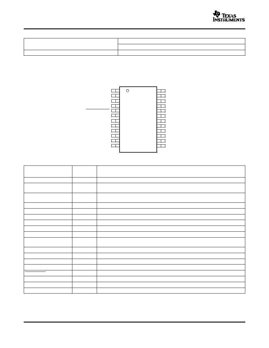
INN
INP
GAIN0
SHUTDOWN
PGND
VCLAMP
BSN
PV
CC
OUTN
OUTN
PGND
V
CC
VREF
BYPASS
COSC
ROSC
AGND
AGND
BSP
PV
CC
OUTP
GAIN1
OUTP
PGND
1
2
3
4
5
6
7
8
9
10
11
12
24
23
22
21
20
19
18
17
16
15
14
13
R3
51
C9
0.22
µ
F
C6
1
µ
F
D1
V
CC
C12
220 pF
C11
1
µ
F
C3
1
µ
F
C4
1
µ
F
V
CC
L2
(Ferrite
Bead)
L1
(Ferrite
Bead)
C15
1 nF
C14
1 nF
D2
R2
51
C8
0.22
µ
F
C5
1
µ
F
C7
10
µ
F
C10
1
µ
F
C1
0.47
µ
F
C2
0.47
µ
F
IN-
IN+
GAIN SELECT
GAIN SELECT
SHUTDOWN
CONTROL
U1
TPA3007D1
V
CC
R1
120 k
TPA3007D1
SLOS418A ≠ SEPTEMBER 2003 ≠ REVISED DECEMBER 2004
6.5-W MONO CLASS-D AUDIO POWER AMPLIFIER
∑
6.5 W Into 8-
Load From 12-V Supply
The TPA3007D1 is a 6.5-W mono bridge-tied load
(10% THD+N)
(BTL) class-D audio power amplifier with high ef-
ficiency, eliminating the need for heat sinks. The
∑
Short Circuit Protection (Short to V
CC
, Short
TPA3007D1 can drive 8-
speakers with only a
to GND, Short Between Outputs)
ferrite bead filter required to reduce EMI.
∑
Third-Generation Modulation Technique:
The gain of the amplifier is controlled by two input
≠ Replaces Large LC Filter With Small,
terminals, GAIN1 and GAIN0. This allows the ampli-
Low-Cost Ferrite Bead Filter in Most
fier to be configured for a gain of 12, 18, 23.6, and 36
Applications
dB. The differential input stage provides high com-
≠ Improved Efficiency
mon mode rejection and improved power supply
rejection.
≠ Improved SNR
∑
Low Supply Current . . . 8 mA Typ at 12 V
The amplifier also includes depop circuitry to reduce
the amount of pop at power-up and when cycling
∑
Shutdown Control . . . <1 µA Typ
SHUTDOWN.
The TPA3007D1 is available in the 24-pin TSSOP
package (PW) and does not require an external heat
∑
LCD Monitors/TVs
sink.
∑
Desktop Replacement Notebook PCs
∑
Hands-Free Car Kits
∑
Powered Speakers
Functional Schematic Diagram
Please be aware that an important notice concerning availability, standard warranty, and use in critical applications of Texas
Instruments semiconductor products and disclaimers thereto appears at the end of this data sheet.
PRODUCTION DATA information is current as of publication date.
Copyright © 2003≠2004, Texas Instruments Incorporated
Products conform to specifications per the terms of the Texas
Instruments standard warranty. Production processing does not
necessarily include testing of all parameters.
www.ti.com
1
2
3
4
5
6
7
8
9
10
11
12
24
23
22
21
20
19
18
17
16
15
14
13
INN
INP
GAIN0
GAIN1
SHUTDOWN
PGND
VCLAMP
BSN
PV
CC
OUTN
OUTN
PGND
V
CC
VREF
BYPASS
COSC
ROSC
AGND
AGND
BSP
PV
CC
OUTP
OUTP
PGND
TPA3007D1
SLOS418A ≠ SEPTEMBER 2003 ≠ REVISED DECEMBER 2004
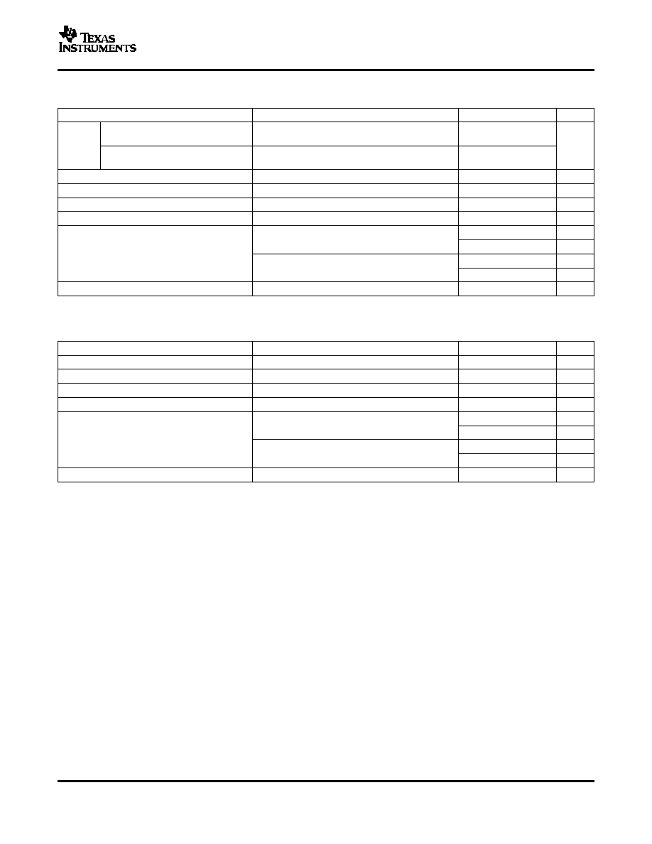
AVAILABLE OPTIONS
PACKAGED DEVICES
T
A
TSSOP (PW)
(1)
-40
∞
C to 85
∞
C
TPA3007D1PW
(1)
The PW package is available taped and reeled. To order a taped and reeled part, add the suffix R to the part number (e.g.,
TPA3007D1PWR).
PW PACKAGE
(TOP VIEW)
Terminal Functions
TERMINAL
I/O
DESCRIPTION
NAME
NO.
AGND
18, 19
Analog ground terminal
Bootstrap terminal for high-side gate drive of negative BTL output (connect a 0.22-µF
BSN
8
I
capacitor with a 51-
resistor in series from OUTN to BSN)
Bootstrap terminal for high-side gate drive of positive BTL output (connect a 0.22-µF
BSP
17
I
capacitor with a 51-
resistor in series from OUTP to BSP)
BYPASS
22
I
Connect 1-µF capacitor to ground for BYPASS voltage filtering
COSC
21
I
Connect a 220-pF capacitor to ground to set oscillation frequency
GAIN0
3
I
Bit 0 of gain control (see Table 2 for gain settings)
GAIN1
4
I
Bit 1 of gain control (see Table 2 for gain settings)
INN
1
I
Negative differential input
INP
2
I
Positive differential input
Negative BTL output, connect Schottky diode from PGND to OUTN for short-circuit
OUTN
10, 11
O
protection
OUTP
14, 15
O
Positive BTL output, connect Schottky diode from PGND to OUTP for short-circuit protection
PGND
6, 12, 13
Power ground
PV
CC
9, 16
I
High-voltage power supply (for output stages)
ROSC
20
I
Connect 120 k
resistor to ground to set oscillation frequency
SHUTDOWN
5
I
Shutdown terminal (active low), TTL compatible, 21-V compliant
V
CC
24
I
Analog high-voltage power supply
VCLAMP
7
O
Connect 1-µF capacitor to ground to provide reference voltage for H-bridge gates
VREF
23
O
5-V internal regulator for control circuitry (connect a 0.1-µF to 1-µF capacitor to ground)
2

www.ti.com
Gate
Drive
_
+
Gate
Drive
_
+
_
+
_
+
Gain
Adjust
Gain
Adjust
Start-Up
Protection
Logic
Short-Circuit
Detect
Thermal
V
CC
OK
Ramp
Generator
Biases
and
References
Gain
2
AGND
VREF
VREF
PV
CC
INN
OUTN
PGND
PV
CC
OUTP
PGND
INP
SHUTDOWN
GAIN1
GAIN0
COSC
ROSC
BYPASS
SD
_
+
_
+
Deglitch
Logic
Deglitch
Logic
V
CC
V
CC
BSP
BSN
Clamp
Reference
VCLAMP
ABSOLUTE MAXIMUM RATINGS
TPA3007D1
SLOS418A ≠ SEPTEMBER 2003 ≠ REVISED DECEMBER 2004
Functional Block Diagram
over operating free-air temperature range (unless otherwise noted)
(1)
UNIT
Supply voltage: V
CC,
PV
CC
-0.3 V to 21 V
Load impedance, R
L
7
Input voltage
SHUTDOWN
-0.3 V to V
CC
+ 0.3 V
GAIN0, GAIN1
-0.3 V to 5.5 V
INN, INP
-0.3 V to 7 V
Continuous total power dissipation
See Dissipation Rating Table
Operating free-air temperature range, T
A
-40
∞
C to 85
∞
C
Operating junction temperature range, T
J
-40
∞
C to 150
∞
C
Storage temperature range, T
stg
-65
∞
C to 85
∞
C
Lead temperature 1,6 mm (1/16 inch) from case for 10 seconds
260
∞
C
(1)
Stresses beyond those listed under "absolute maximum ratings" may cause permanent damage to the device. These are stress ratings
only, and functional operation of the device at these or any other conditions beyond those indicated under "recommended operating
conditions" is not implied. Exposure to absolute-maximum-rated conditions for extended periods may affect device reliability.
DISSIPATION RATING TABLE
PACKAGE
T
A
25
∞
C
DERATING FACTOR
T
A
= 70
∞
C
T
A
= 85
∞
C
PW
1.43 W
11.45 mW/
∞
C
(1)
0.915 W
0.744 W
(1)
Based on High-K board
3

www.ti.com
RECOMMENDED OPERATING CONDITIONS
ELECTRICAL CHARACTERISTICS
TPA3007D1
SLOS418A ≠ SEPTEMBER 2003 ≠ REVISED DECEMBER 2004
MIN
MAX
UNIT
Supply voltage, V
CC,
PV
CC
R
L
7.0
(1)
8
18
V
Load impedance, R
L
7.0
High-level input voltage, V
IH
GAIN0, GAIN1, SHUTDOWN
2
V
Low-level input voltage, V
IL
GAIN0, GAIN1, SHUTDOWN
0.8
V
Operating free-air temperature, T
A
40
85
∞
C
Operating junction temperature, T
J
(2)
125
∞
C
(1)
The TPA3007D1 must not be used with any speaker or load (including speaker with output filter) that could vary below 7.0
over the
audio frequency band.
(2)
Continuous operation above the recommended junction temperature may result in reduced reliability and/or lifetime of the device. The
junction temperature is controlled by the thermal design of the application and should be carefully considered in high power dissipation
applications. See the thermal considerations section on page 14 for recommendations on improving the thermal performance of your
application.
T
A
= 25
∞
C, PV
CC
= V
CC
= 12 V (unless otherwise noted)
PARAMETERS
TEST CONDITIONS
MIN
TYP
MAX UNIT
V
I
= 0 V, A
V
= 12 dB, 18, 23.6 dB
50
Output offset voltage (measured differen-
|V
OS
|
mV
tially)
V
I
= 0 V, A
V
= 36 dB
100
PSRR
Power supply rejection ratio
PV
CC
= 11.5 V to 12.5 V
73
dB
|I
IH
|
High-level input current
PV
CC
= 12 V, V
I
= PV
CC
1
µA
|I
IL
|
Low-level input current
PV
CC
= 12 V, V
I
= 0 V
1
µA
SHUTDOWN = 2.0 V, No load
8
15
mA
I
CC
Supply current
SHUTDOWN = V
CC
, V
CC
= 18 V,P
O
= 6.5 W, R
L
=
0.42
A
8
I
CC(SD)
Supply current, shutdown mode
SHUTDOWN = 0.8 V
1
2
µA
f
s
Switching frequency
R
OSC
= 120 k
, C
OSC
= 220 pF
250
kHz
r
ds(on)
Output transistor on resistance (total)
I
O
= 1 A, T
J
= 25
∞
C
1.4
GAIN1 = 0.8 V, GAIN0 = 0.8 V
10.9
12
12.8
dB
GAIN1 = 0.8 V, GAIN0 = 2 V
17.1
18
18.5
dB
G
Gain
GAIN1 = 2 V, GAIN0 = 0.8 V
23
23.6
24.3
dB
GAIN1 = 2 V, GAIN0 = 2 V
33.9
36
36.5
dB
4
www.ti.com
OPERATING CHARACTERISTICS
OPERATING CHARACTERISTICS
TPA3007D1
SLOS418A ≠ SEPTEMBER 2003 ≠ REVISED DECEMBER 2004
PV
CC
= V
CC
= 12 V, Gain = 12 dB, T
A
= 25
∞
C (unless otherwise noted)
PARAMETER
TEST CONDITIONS
MIN
TYP
MAX
UNIT
Continuous output power at 10%
f = 1 kHz, R
L
= 8
6.5
THD+N
P
O
W
Continuous output power at 1%
f = 1 kHz, R
L
= 8
5.0
THD+N
THD + N
Total harmonic distortion plus noise
P
O
= 3.25 W, R
L
= 8
, f = 1 kHz
0.19%
B
OM
Maximum output power bandwidth
THD = 1%
20
kHz
k
SVR
Supply ripple rejection ratio
f = 1 kHz, C
(BYPASS)
= 1 µF
70
dB
SNR
Signal-to-noise ratio
P
O
= 3.25 W, R
L
= 8
97
dB
86
µV(rms)
C
(BYPASS)
= 1 µF, f = 20 Hz to 22 kHz, No weighting
filter used
81
dBV
V
n
Noise output voltage
66
µV(rms)
C
(BYPASS)
= 1 µF, f = 20 Hz to 22 kHz, A-weighted
filter
84
dBV
Z
i
Input impedance
See Table 2, page 14
>23
k
PV
CC
= V
CC
= 18 V, Gain = 12 dB, T
A
= 25
∞
C (unless otherwise noted)
PARAMETER
TEST CONDITIONS
MIN
TYP
MAX
UNIT
THD + N
Total harmonic distortion plus noise
P
O
= 3.25 W, R
L
= 8
, f = 1 kHz
0.16%
B
OM
Maximum output power bandwidth
THD = 1%
20
kHz
k
SVR
Supply ripple rejection ratio
f = 1 kHz, C
BYPASS
= 1 µF
70
dB
SNR
Signal-to-noise ratio
P
O
= 3.25 W, R
L
= 8
97
dB
86
µV(rms)
C
(BYPASS)
= 1 µF, f = 20 Hz to 20 kHz, No weighting
filter used
81
dBV
V
n
Noise output voltage
66
µV(rms)
C
(BYPASS)
= 1 µF, f = 20 Hz to 22 kHz, A-weighted
filter
84
dBV
Z
i
Input impedance
See Table 2, page 14
>23
k
5