 | –≠–ª–µ–∫—Ç—Ä–æ–Ω–Ω—ã–π –∫–æ–º–ø–æ–Ω–µ–Ω—Ç: TPIC6595N | –°–∫–∞—á–∞—Ç—å:  PDF PDF  ZIP ZIP |
TPIC6595
POWER LOGIC 8-BIT SHIFT REGISTER
SLIS010A ≠ APRIL 1992 ≠ REVISED OCTOBER 1995
1
POST OFFICE BOX 655303
∑
DALLAS, TEXAS 75265
D
Low r
DS(on)
. . . 1.3
Typical
D
Avalanche Energy . . . 75 mJ
D
Eight Power DMOS Transistor Outputs of
250-mA Continuous Current
D
1.5-A Pulsed Current Per Output
D
Output Clamp Voltage at 45 V
D
Devices Are Cascadable
D
Low Power Consumption
description
The TPIC6595 is a monolithic, high-voltage, high-
current power 8-bit shift register designed for use
in systems that require relatively high load power.
The device contains a built-in voltage clamp on
the outputs for inductive transient protection.
Power driver applications include relays, sole-
noids, and other medium-current or high-voltage
loads.
This device contains an 8-bit serial-in, parallel-out
shift register that feeds an 8-bit D-type storage
register. Data transfers through both the shift and
storage registers on the rising edge of the
shift-register clock (SRCK) and the register clock
(RCK) respectively. The storage register transfers
data to the output buffer when shift-
register clear (SRCLR) is high. When SRCLR is
low, the input shift register is cleared. When output
enable (G) is held high, all data in the output
buffers is held low and all drain outputs are off.
When G is held low, data from the storage register
is transparent to the output buffers. The serial
output (SER OUT) allows for cascading of the
data from the shift register to additional devices.
Outputs are low-side, open-drain DMOS
transistors with output ratings of 45 V and 250-mA
continuous sink current capability. When data in the output buffers is low, the DMOS-transistor outputs are off.
When data is high, the DMOS-transistor outputs have sink current capability.
Separate power and logic level ground pins are provided to facilitate maximum system flexibility. Pins 1, 10, 11,
and 20 are internally connected, and each pin must be externally connected to the power system ground in order
to minimize parasitic inductance. A single-point connection between pin 19, logic ground (LGND), and pins 1,
10, 11, and 20, power grounds (PGND), must be externally made in a manner that reduces crosstalk between
the logic and load circuits.
The TPIC6595 is characterized for operation over the operating case temperature range of ≠ 40
∞
C to 125
∞
C.
Copyright
©
1995, Texas Instruments Incorporated
PRODUCTION DATA information is current as of publication date.
Products conform to specifications per the terms of Texas Instruments
standard warranty. Production processing does not necessarily include
testing of all parameters.
This symbol is in accordance with ANSI/IEEE Std 91-1984
and IEC Publication 617-12.
1
2
3
4
5
6
7
8
9
10
20
19
18
17
16
15
14
13
12
11
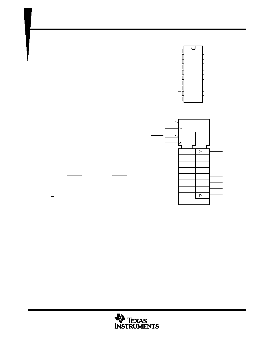
PGND
V
CC
SER IN
DRAIN0
DRAIN1
DRAIN2
DRAIN3
SRCLR
G
PGND
PGND
LGND
SER OUT
DRAIN7
DRAIN6
DRAIN5
DRAIN4
SRCK
RCK
PGND
DW OR N PACKAGE
(TOP VIEW)
logic symbol
2
SRG8
9
12
8
13
3
EN3
C2
R
C1
1D
G
RCK
SRCLR
SRCK
SER IN
4
6
5
14
7
16
15
18
17
DRAIN0
DRAIN1
DRAIN2
DRAIN3
DRAIN4
DRAIN5
DRAIN6
DRAIN7
SER OUT
2
TPIC6595
POWER LOGIC 8-BIT SHIFT REGISTER
SLIS010A ≠ APRIL 1992 ≠ REVISED OCTOBER 1995
2
POST OFFICE BOX 655303
∑
DALLAS, TEXAS 75265
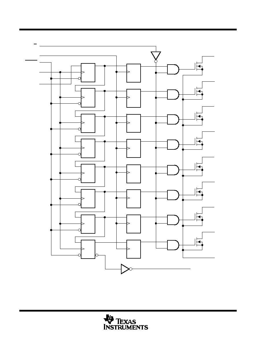
logic diagram (positive logic)
G
RCK
SRCLR
SRCK
SER IN
CLR
D
C1
D
C2
SER OUT
4
DRAIN0
5
DRAIN1
1, 10, 11, 20
PGND
6
DRAIN2
7
DRAIN3
14
DRAIN4
15
DRAIN5
16
DRAIN6
17
DRAIN7
9
8
3
12
13
18
CLR
D
C1
CLR
D
C1
CLR
D
C1
CLR
D
C1
CLR
D
C1
CLR
D
C1
CLR
D
C1
D
C2
D
C2
D
C2
D
C2
D
C2
D
C2
D
C2

TPIC6595
POWER LOGIC 8-BIT SHIFT REGISTER
SLIS010A ≠ APRIL 1992 ≠ REVISED OCTOBER 1995
3
POST OFFICE BOX 655303
∑
DALLAS, TEXAS 75265
schematic of inputs and outputs
EQUIVALENT OF EACH INPUT
TYPICAL OF ALL DRAIN OUTPUTS
VCC
Input
LGND
PGND
DRAIN
45 V
12 V
25 V
12 V
LGND
absolute maximum ratings over recommended operating case temperature range (unless
otherwise noted)
Logic supply voltage, V
CC
(see Note NO TAG)
7 V
. . . . . . . . . . . . . . . . . . . . . . . . . . . . . . . . . . . . . . . . . . . . . . . .
Logic input voltage range, V
I
≠ 0.3 V to 7 V
. . . . . . . . . . . . . . . . . . . . . . . . . . . . . . . . . . . . . . . . . . . . . . . . . . . . . . . .
Power DMOS drain-to-source voltage, V
DS
(see Note NO TAG)
45 V
. . . . . . . . . . . . . . . . . . . . . . . . . . . . . . . . .
Continuous source-drain diode anode current
1 A
. . . . . . . . . . . . . . . . . . . . . . . . . . . . . . . . . . . . . . . . . . . . . . . . . .
Pulsed source-drain diode anode current
2 A
. . . . . . . . . . . . . . . . . . . . . . . . . . . . . . . . . . . . . . . . . . . . . . . . . . . . . .
Pulsed drain current, each output, all outputs on, I
Dn,
T
A
= 25
∞
C (see Note NO TAG)
750 mA
. . . . . . . . . . . .
Continuous drain current, each output, all outputs on, I
Dn,
T
A
= 25
∞
C 250
mA
. . . . . . . . . . . . . . . . . . . . . . . . . .
Peak drain current single output, I
DM,
T
A
= 25
∞
C (see Note NO TAG)
2 A
. . . . . . . . . . . . . . . . . . . . . . . . . . . . . .
Single-pulse avalanche energy, E
AS
(see NO TAG)
75
mJ
. . . . . . . . . . . . . . . . . . . . . . . . . . . . . . . . . . . . . . . . . . .
Avalanche current, I
AS
(see Note NO TAG)
1
A
. . . . . . . . . . . . . . . . . . . . . . . . . . . . . . . . . . . . . . . . . . . . . . . . . . . .
Continuous total power dissipation
See Dissipation Rating Table
. . . . . . . . . . . . . . . . . . . . . . . . . . . . . . . . . . . . .
Operating virtual junction temperature range, T
J
≠ 40
∞
C to 150
∞
C
. . . . . . . . . . . . . . . . . . . . . . . . . . . . . . . . . . . . .
Storage temperature range, T
stg
≠ 65
∞
C to 150
∞
C
. . . . . . . . . . . . . . . . . . . . . . . . . . . . . . . . . . . . . . . . . . . . . . . . . . .
Lead temperature 1,6 mm (1/16 inch) from case for 10 seconds
260
∞
C
. . . . . . . . . . . . . . . . . . . . . . . . . . . . . . .
Stresses beyond those listed under "absolute maximum ratings" may cause permanent damage to the device. These are stress ratings only and
functional operation of the device at these or any other conditions beyond those indicated under "recommended operating conditions" is not
implied. Exposure to absolute-maximum-rated conditions for extended periods may affect device reliability.
NOTES:
1. All voltage values are with respect to LGND and PGND.
2. Each power DMOS source is internally connected to PGND.
3. Pulse duration
100
µ
s, duty cycle
2 %
4. DRAIN supply voltage = 15 V, starting junction temperature (TJS) = 25
∞
C, L = 100 mH, IAS = 1 A (see NO TAG).
DISSIPATION RATING TABLE
PACKAGE
TA
25
∞
C
POWER RATING
DERATING FACTOR
ABOVE TA = 25
∞
C
TA = 125
∞
C
POWER RATING
DW
1125 mW
9.0 mW/
∞
C
225 mW
N
1150 mW
9.2 mW/
∞
C
230 mW

TPIC6595
POWER LOGIC 8-BIT SHIFT REGISTER
SLIS010A ≠ APRIL 1992 ≠ REVISED OCTOBER 1995
4
POST OFFICE BOX 655303
∑
DALLAS, TEXAS 75265
recommended operating conditions over recommended operating temperature range (unless
otherwise noted)
MIN
MAX
UNIT
Logic supply voltage, VCC
4.5
5.5
V
High-level input voltage, VIH
0.85 VCC
V
Low-level input voltage, VIL
0.15 VCC
V
Pulsed drain output current, TC = 25
∞
C, VCC = 5 V (see Notes 3 and 5)
≠ 1.8
1.5
A
Setup time, SER IN high before SRCK
, tsu (see NO TAG)
10
ns
Hold time, SER IN high after SRCK
, th (see NO TAG)
10
ns
Pulse duration, tw (see NO TAG)
20
ns
Operating case temperature, TC
≠ 40
125
∞
C
electrical characteristics, V
CC
= 5 V, T
C
= 25
∞
C (unless otherwise noted)
PARAMETER
TEST CONDITIONS
MIN
TYP
MAX
UNIT
V(BR)DSX Drain-source breakdown voltage
ID = 1 mA
45
V
VSD
Source-drain diode forward voltage
IF = 250 mA,
See Note 3
0.85
1
V
VOH
High-level output voltage,
IOH = ≠ 20 mA, VCC = 4.5 V
4.4
4.49
V
VOH
g
g ,
SER OUT
IOH = ≠ 4 mA, VCC = 4.5 V
4.1
4.3
V
VOL
Low-level output voltage, SER
IOH = 20 mA, VCC = 4.5 V
0.002
0.1
V
VOL
g ,
OUT
IOH = 4 mA,
VCC = 4.5 V
0.2
0.4
V
V(hys)
Input hysteresis
VDS = 15 V
1.3
V
IIH
High-level input current
VCC = 5.5 V,
VI = VCC
1
µ
A
IIL
Low-level input current
VCC = 5.5 V,
VI = 0
≠ 1
µ
A
ICCL
Logic supply current
IO = 0,
All inputs low
15
100
µ
A
ICC(FRQ)
Logic supply current frequency
fSRCK = 5 MHz, IO = 0, CL = 30 pF,
See Figures 1, 2, and 6
0.6
5
mA
IN
Nominal current
VDS(on) = 0.5 V,
IN = ID,
TC = 85
∞
C
See Notes 5, 6, and 7
250
mA
IDSX
Off state drain current
VDS = 40 V
0.05
1
µ
A
IDSX
Off-state drain current
VDS = 40 V,
TC = 125
∞
C
0.15
5
µ
A
ID = 250 mA,
VCC = 4.5 V
1.3
2
rDS(on)
Static drain-source on-state
resistance
ID = 250 mA,
TC = 125
∞
C,
VCC = 4.5 V
See Notes 5 and 6
and Figures 9 and 10
2
3.2
ID = 500 mA,
VCC = 4.5 V NO TAG
1.3
2
switching characteristics, V
CC
= 5 V, T
C
= 25
∞
C
PARAMETER
TEST CONDITIONS
MIN
TYP
MAX
UNIT
tPLH
Propagation delay time, low-to-high-level output from G
650
ns
tPHL
Propagation delay time, high-to-low-level output from G
CL = 30 pF,
ID = 250 mA,
150
ns
tr
Rise time, drain output
L
,
D
,
See Figures 1 and 2
750
ns
tf
Fall time, drain output
425
ns
ta
Reverse-recovery-current rise time
IF = 250 mA,
di/dt = 20 A/
µ
s,
100
ns
trr
Reverse-recovery time
F
,
µ
,
See Notes 5 and 6 and Figure 3
300
ns
NOTES:
3. Pulse duration
100
µ
s, duty cycle
2%
5. Technique should limit TJ ≠ TC to 10
∞
C maximum.
6. These parameters are measured with voltage-sensing contacts separate from the current-carrying contacts.
7. Nominal current is defined for a consistent comparison between devices from different sources. It is the current that produces a
voltage drop of 0.5 V at TC = 85
∞
C.

TPIC6595
POWER LOGIC 8-BIT SHIFT REGISTER
SLIS010A ≠ APRIL 1992 ≠ REVISED OCTOBER 1995
5
POST OFFICE BOX 655303
∑
DALLAS, TEXAS 75265
thermal resistance
PARAMETER
TEST CONDITIONS
MIN
MAX
UNIT
R
JA
Thermal resistance junction to ambient
DW package
All 8 outputs with equal power
111
∞
C/W
R
JA
Thermal resistance, junction-to-ambient
N package
All 8 outputs with equal power
108
∞
C/W
PARAMETER MEASUREMENT INFORMATION
TEST CIRCUIT
5 V
VCC
DRAIN
LGND
SRCLR
SER IN
RL = 95
CL = 30 pF
(see Note B)
VOLTAGE WAVEFORMS
G
Output
SRCK
RCK
Word
Generator
(see Note A)
7
6
5
4
3
2
1
0
5 V
SRCK
5 V
G
5 V
SER IN
RCK
SRCLR
5 V
5 V
DUT
PGND
24 V
DRAIN1
24 V
0 V
0 V
0 V
0.5 V
0 V
19
1, 10, 11, 20
8
13
3
12
9
0 V
4 ≠7,
14 ≠17
ID
2
Figure 1. Resistive Load Operation
4 ≠7,
14 ≠17
TEST CIRCUIT
SWITCHING TIMES
G
5 V
50%
24 V
0.5 V
90%
10%
tPLH
tr
50%
90%
10%
tPHL
tf
SRCK
5 V
50%
SER IN
5 V
50%
50%
tsu
th
tw
INPUT SETUP AND HOLD WAVEFORMS
5 V
24 V
VCC
DRAIN
LGND
SRCLR
SER IN
RL = 95
CL = 30 pF
(see Note B)
G
Output
SRCK
RCK
DUT
PGND
Output
Word
Generator
(see Note A)
19
1, 10, 11, 20
8
13
3
12
9
0 V
0 V
0 V
ID
2
Figure 2. Test Circuit, Switching Times, and Voltage Waveforms
NOTES: A. Outputs DRAIN 1, 2, 5, and 6 low (PGND), all other DRAIN outputs are at 24 V. The word generator has the following characteristics:
tr
10 ns, tf
10 ns, tw = 300 ns, pulsed repetition rate (PRR) = 5 kHz, ZO = 50
.
B. CL includes probe and jig capacitance.