www.ti.com
FEATURES
DESCRIPTION
APPLICATIONS
V
BAT
RESET
MR
PFO
8
7
6
5
1
2
3
4
V
OUT
V
DD
GND
PFI
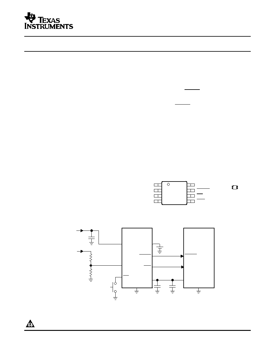
DGK PACKAGE
(TOP VIEW)
ACTUAL SIZE
3,05 mm x 4,98 mm
V
DD
V
BAT
PFI
Backup
Battery
RESET
PFO
V
OUT
GND
R
x
R
y
External
Source
0.1
µ
F
Power
Supply
GND
RESET
I/O
V
CC
Switchover
Capacitor
0.1
µ
F
TPS3619
TPS3620
Microcontroller
or
Microprocessor
Manual
Reset
MR
TPS3619-33, TPS3619-50
TPS3620-33, TPS3620-50
SLVS387E ≠ APRIL 2001 ≠ REVISED SEPTEMBER 2004
BACKUP-BATTERY SUPERVISORS FOR RAM RETENTION
∑
Supply Current of 40 µA (Max)
The TPS3619 and TPS3620 families of supervisory
circuits monitor and control processor activity by
∑
Battery-Supply Current of 100 nA (Max)
providing backup-battery switchover for data retention
∑
Precision Supply Voltage Monitor 3.3 V, 5 V,
of CMOS RAM.
Other Options on Request
During power on, RESET is asserted when the
∑
Backup-Battery Voltage Can Exceed V
DD
supply voltage (V
DD
or V
BAT
) becomes higher than 1.1
∑
Power On Reset Generator With Fixed 100-ms
V. Thereafter, the supply voltage supervisor monitors
Reset Delay Time
V
DD
and keeps RESET output active as long as V
DD
∑
Voltage Monitor For Power-Fail or
remains below the threshold voltage (V
IT
). An internal
timer delays the return of the output to the inactive
Low-Battery Monitoring
state (high) to ensure proper system reset. The delay
∑
Battery Freshness Seal (TPS3619)
time starts after V
DD
has risen above V
IT
. When the
∑
Pin-For-Pin Compatible With MAX819,
supply voltage drops below V
IT,
the output becomes
MAX703, and MAX704
active (low) again.
∑
8-Pin MSOP Package
The product spectrum is designed for supply voltages
∑
Temperature Range -40
∞
C to 85
∞
C
of 3.3 V and 5 V. The TPS3619 and TPS3620 are
available in an 8-pin MSOP package and are
characterized for operation over a temperature range
of -40
∞
C to 85
∞
C.
∑
Fax Machines
∑
Set-Top Boxes
∑
Advanced Voice Mail Systems
∑
Portable Battery-Powered Equipment
∑
Computer Equipment
∑
Advanced Modems
∑
Automotive Systems
∑
Portable Long-Time Monitoring Equipment
∑
Point-of-Sale Equipment
TYPICAL OPERATING CIRCUIT
Please be aware that an important notice concerning availability, standard warranty, and use in critical applications of Texas
Instruments semiconductor products and disclaimers thereto appears at the end of this data sheet.
PRODUCTION DATA information is current as of publication date.
Copyright © 2001≠2004, Texas Instruments Incorporated
Products conform to specifications per the terms of the Texas
Instruments standard warranty. Production processing does not
necessarily include testing of all parameters.
www.ti.com
STANDARD AND APPLICATION SPECIFIC VERSIONS
TPS361
9 ≠ 33
DGK
R
Reel
Nominal Supply Voltage
Package
Functionality
Family
ABSOLUTE MAXIMUM RATINGS
TPS3619-33, TPS3619-50
TPS3620-33, TPS3620-50
SLVS387E ≠ APRIL 2001 ≠ REVISED SEPTEMBER 2004
This integrated circuit can be damaged by ESD. Texas Instruments recommends that all integrated
circuits be handled with appropriate precautions. Failure to observe proper handling and installation
procedures can cause damage.
ESD damage can range from subtle performance degradation to complete device failure. Precision
integrated circuits may be more susceptible to damage because very small parametric changes could
cause the device not to meet its published specifications.
PACKAGE INFORMATION
SPECIFIED TEMPERATURE
PACKAGE
TRANSPORT MEDIA,
PRODUCT
ORDERING NUMBER
RANGE
MARKING
QUANTITY
TPS3619-33DGK
Tube, 80
TPS3619-33
AFL
TPS3619-33DGKR
Tape and Reel, 2500
TPS3619-50DGK
Tube, 80
TPS3619-50
AFM
TPS3619-50DGKR
Tape and Reel, 2500
-40
∞
C to 85
∞
C
TPS3620-33DGK
Tape and Reel, 250
TPS3620-33
ANL
TPS3620-33DGKR
Tape and Reel, 2500
TPS3620-50DGK
(1)
Tape and Reel, 250
TPS3620-50
ANM
TPS3620-50DGKR
(1)
Tape and Reel, 2500
(1)
Available Q4, 2004.
DEVICE NAME
NOMINAL VOLTAGE
(1)
, V
NOM
TPS3619-33 DGK
3.3 V
TPS3619-50 DGK
5.0 V
TPS3620-33 DGK
3.3 V
TPS3620-50 DGK
5.0 V
(1)
For other threshold voltage versions, contact the local TI sales
office for availability and lead-time.
over operating free-air temperature (unless otherwise noted)
(1)
UNIT
Supply voltage:
V
DD
(see
(2)
)
7 V
MR and PFI pins (see
(2)
)
-0.3 V to (V
DD
+ 0.3 V)
Continuous output current:
V
OUT
, I
O
400 mA
All other pins, I
O
(see
(2)
)
±
10 mA
Continuous total power dissipation
See Dissipation Rating Table
Operating free-air temperature range, T
A
-40
∞
C to 85
∞
C
Storage temperature range, T
stg
-65
∞
C to 150
∞
C
Lead temperature soldering 1,6 mm (1/16 inch) from case for 10 seconds
260
∞
C
(1)
Stresses beyond those listed under absolute maximum ratings may cause permanent damage to the device. These are stress ratings
only, and functional operation of the device at these or any other conditions beyond those indicated under recommended operating
conditions is not implied. Exposure to absolute-maximum-rated conditions for extended periods may affect device reliability.
(2)
All voltage values are with respect to GND. For reliable operation, the device must not be operated at 7 V for more than t=1000h
continuously.
2
www.ti.com
DISSIPATION RATING TABLE
RECOMMENDED OPERATING CONDITIONS
ELECTRICAL CHARACTERISTICS
TPS3619-33, TPS3619-50
TPS3620-33, TPS3620-50
SLVS387E ≠ APRIL 2001 ≠ REVISED SEPTEMBER 2004
T
A
< 25
∞
C
DERATING FACTOR
T
A
= 70
∞
C
T
A
= 85
∞
C
PACKAGE
POWER RATING
ABOVE T
A
= 25
∞
C
POWER RATING
POWER RATING
DGK
470 mW
3.76 mW/
∞
C
301 mW
241 mW
at specified temperature range
MIN
MAX
UNIT
Supply voltage, V
DD
1.65
5.5
V
Battery supply voltage, V
BAT
1.5
5.5
V
Input voltage, V
I
0
V
DD
+ 0.3
V
High-level input voltage, V
IH
0.7 x V
DD
V
Low-level input voltage, V
IL
0.3 x V
DD
V
Continuous output current at V
OUT
, I
O
300
mA
Input transition rise and fall rate at MR
100
ns/V
Slew rate at V
DD
or V
BAT
,
t/
V
1
V/µs
Operating free-air temperature range, T
A
-40
85
∞
C
over recommended operating conditions (unless otherwise noted)
PARAMETER
TEST CONDITIONS
MIN
TYP
MAX
UNIT
V
DD
= 1.8 V,
I
OH
= -400 µA
V
DD
- 0.2 V
RESET
V
DD
= 3.3 V,
I
OH
= -2 mA
V
DD
- 0.4 V
V
V
DD
= 5 V,
I
OH
= -3 mA
V
DD
- 0.4 V
V
OH
High-level output voltage
V
DD
= 1.8 V,
I
OH
= -20 µA
V
DD
- 0.3 V
PFO
V
DD
= 3.3 V,
I
OH
= -80 µA
V
DD
- 0.4 V
V
V
DD
= 5 V,
I
OH
= -120 µA
V
DD
- 0.4 V
V
DD
= 1.8 V,
I
OL
= -400 µA
0.2
V
OL
Low-level output voltage
RESET PFO
V
DD
= 3.3 V,
I
OL
= 2 mA
0.4
V
V
DD
= 5 V,
I
OL
= 3 mA
0.4
I
OL
= 20 µA, V
BAT
> 1.1 V or
V
res
Powerup reset voltage (see
(1)
)
0.4
V
V
DD
> 1.1 V
I
OUT
= 8.5 mA,
V
DD
= 1.8 V
V
DD
- 50 V
V
BAT
= 0 V
I
OUT
= 125 mA,
Normal mode
V
DD
= 3.3 V
V
DD
- 150 V
V
V
BAT
= 0 V
I
OUT
= 200 mA,
V
OUT
V
DD
= 5 V
V
DD
- 200 V
V
BAT
= 0 V
I
OUT
= 0.5 mA,
V
DD
= 0 V
V
BAT
- 20 mV
V
BAT
= 1.5 V
Battery-backup mode
V
I
OUT
= 7.5 mA,
V
BAT
- 113 mV
V
BAT
= 3.3 V
V
DD
to V
OUT
on-resistance
V
DD
= 5 V
0.6
1
r
DS(on)
V
BAT
to V
OUT
on-resistance
V
DD
= 3.3 V
8
15
TPS3619-33
2.88
2.93
3
V
IT-
Negative-going input
TPS3619-50
T
A
= -40
∞
C to 85
∞
C
4.46
4.55
4.64
V
threshold voltage (see
(2)
)
V
PFI
PFI
1.13
1.15
1.17
(1)
The lowest supply voltage at which RESET becomes active. t
r,VDD
15 µs/V.
(2)
To ensure the best stability of the threshold voltage, a bypass capacitor (ceramic, 0.1 µF) should be placed near the supply terminals.
3
www.ti.com
TIMING REQUIREMENTS
SWITCHING CHARACTERISTICS
TPS3619-33, TPS3619-50
TPS3620-33, TPS3620-50
SLVS387E ≠ APRIL 2001 ≠ REVISED SEPTEMBER 2004
ELECTRICAL CHARACTERISTICS (continued)
over recommended operating conditions (unless otherwise noted)
PARAMETER
TEST CONDITIONS
MIN
TYP
MAX
UNIT
1.65 V < V
IT
< 2.5 V
20
V
IT
2.5 V < V
IT
< 3.5 V
40
3.5 V < V
IT
< 5.5 V
60
V
hys
Hysteresis
mV
PFI
12
VBSW (see
V
DD
= 1.8 V
55
(3)
)
I
IH
High-level input current
MR = 0.7 x V
DD
-33
-76
MR
V
DD
= 5 V
µA
I
IL
Low-level input current
MR = 0 V
-110
-255
I
I
Input current
PFI
-25
25
nA
V
DD
= 1.8 V
-0.3
I
OS
Short-circuit current
PFO
PFO = 0 V
V
DD
= 3.3 V
-1.1
mA
V
DD
= 5 V
-2.4
V
OUT
= V
DD
40
I
DD
V
DD
supply current
µA
V
OUT
= V
BAT
40
V
OUT
= V
DD
-0.1
0.1
I
(BAT)
V
BAT
supply current
µA
V
OUT
= V
BAT
0.5
C
i
Input capacitance
V
I
= 0 V to 5 V
5
pF
(3)
For V
DD
< 1.6 V, V
OUT
switches to V
BAT
regardless of V
BAT
.
at R
L
= 1 M
, C
L
= 50 pF, T
A
= -40
∞
C to 85
∞
C
PARAMETER
TEST CONDITIONS
MIN
TYP
MAX
UNIT
at V
DD
V
IH
= V
IT
+ 0.2 V, V
IL
= V
IT
- 0.2 V
6
µs
t
w
Pulse width
at MR
V
DD
= V
IT
+ 0.2 V, V
IL
= 0.3 x V
DD
, V
IH
= 0.7 x V
DD
100
ns
at R
L
= 1 M
, C
L
= 50 pF, T
A
= -40
∞
C to 85
∞
C
PARAMETER
TEST CONDITIONS
MIN
TYP
MAX
UNIT
V
DD
V
IT
+ 0.2 V, MR
0.7 x V
DD
t
d
Delay time
60
100
140
ms
See timing diagram
V
DD
to RESET
V
IL
= V
IT
- 0.2 V, V
IH
= V
IT
+ 0.2 V
2
5
Propagation (delay) time,
PFI to PFO delay
V
IL
= V
PFI
- 0.2 V, V
IH
= V
PFI
+ 0.2 V
3
5
t
PHL
µs
high-to-low level output
V
DD
V
IT
+ 0.2 V, V
IL
= 0.3 x V
DD
,
0.1
1
MR to RESET
V
IH
= 0.7 x V
DD
4
www.ti.com
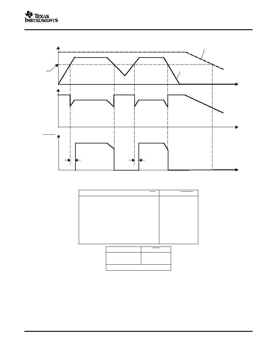
V
IT
V
BAT
V
DD
V
OUT
RESET
t
d
t
t
t
t
d
TPS3619-33, TPS3619-50
TPS3620-33, TPS3620-50
SLVS387E ≠ APRIL 2001 ≠ REVISED SEPTEMBER 2004
TIMING DIAGRAM
FUNCTION TABLE
V
DD
> V
IT
V
DD
> V
BAT
MR
V
OUT
RESET
0
0
0
V
BAT
0
0
0
1
V
BAT
0
0
1
0
V
DD
0
0
1
1
V
DD
0
1
0
0
V
DD
0
1
0
1
V
DD
1
1
1
0
V
DD
0
1
1
1
V
DD
1
PFI > V
PFI
PFO
0
0
1
1
CONDITION.: V
DD
> V
DD
_MIN
5