TPS3820 xx, TPS3823 xx, TPS3824 xx, TPS3825 xx, TPS3828 xx
PROCESSOR SUPERVISORY CIRCUITS
SLVS165E ≠ APRIL 1998 ≠ REVISED DECEMBER 2002
1
POST OFFICE BOX 655303
∑
DALLAS, TEXAS 75265
features
D
Power-On Reset Generator With Fixed
Delay Time of 200 ms (TPS3823/4/5/8)
or 25 ms (TPS3820)
D
Manual Reset Input (TPS3820/3/5/8)
D
Reset Output Available in Active-Low
(TPS3820/3/4/5), Active-High (TPS3824) and
Open-Drain (TPS3828)
D
Supply Voltage Supervision Range
2.5 V, 3 V, 3.3 V, 5 V
D
Watchdog Timer (TPS3820/3/4/8)
D
Supply Current of 15
µ
A (Typ)
D
SOT23-5 Package
D
Temperature Range . . . ≠40
∞
C to 85
∞
C
applications
D
Applications Using DSPs, Microcontrollers,
or Microprocessors
D
Industrial Equipment
D
Programmable Controls
D
Automotive Systems
D
Portable/Battery-Powered Equipment
D
Intelligent Instruments
D
Wireless Communications Systems
D
Notebook/Desktop Computers
description
The TPS382x family of supervisors provides
circuit initialization and timing supervision,
primarily for DSP and processor-based systems.
During power-on, RESET is asserted when
supply voltage V
DD
becomes higher than 1.1 V.
Thereafter, the supply voltage supervisor moni-
tors V
DD
and keeps RESET active as long as V
DD
remains below the threshold voltage V
IT≠
.
An internal timer delays the return of the output to the inactive state (high) to ensure proper system reset. The
delay time, t
d
, starts after V
DD
has risen above the threshold voltage V
IT≠
. When the supply voltage drops below
the threshold voltage V
IT≠
, the output becomes active (low) again. No external components are required. All
the devices of this family have a fixed-sense threshold voltage V
IT≠
set by an internal voltage divider.
Please be aware that an important notice concerning availability, standard warranty, and use in critical applications of
Texas Instruments semiconductor products and disclaimers thereto appears at the end of this data sheet.
Copyright
2002, Texas Instruments Incorporated
This document contains information on products in more than one phase
of development. The status of each device is indicated on the page(s)
specifying its electrical characteristics.
3
2
4
5
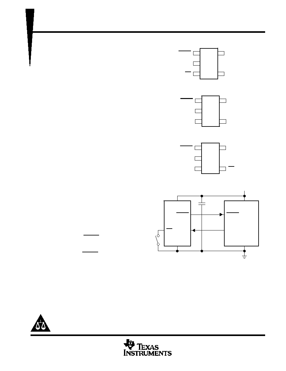
TPS3820, TPS3823, TPS3828 . . . DBV PACKAGE
(TOP VIEW)
1
RESET
GND
MR
VDD
WDI
3
2
4
5
TPS3825 . . . DBV PACKAGE
(TOP VIEW)
1
RESET
GND
RESET
VDD
MR
3
2
4
5
TPS3824 . . . DBV PACKAGE
(TOP VIEW)
1
RESET
GND
RESET
VDD
WDI
RESET
MR
WDI
100 nF
VDD
GND
TPS3823-33
VDD
RESET
I/O
GND
MSP430C325
3.3 V
typical application

TPS3820 xx, TPS3823 xx, TPS3824 xx, TPS3825 xx, TPS3828 xx
PROCESSOR SUPERVISORY CIRCUITS
SLVS165E ≠ APRIL 1998 ≠ REVISED DECEMBER 2002
2
POST OFFICE BOX 655303
∑
DALLAS, TEXAS 75265
description (continued)
The TPS3820/3/5/8 devices incorporate a manual reset input, MR. A low level at MR causes RESET to become
active. The TPS3824/5 devices include a high-level output RESET. TPS3820/3/4/8 have a watchdog timer that
is periodically triggered by a positive or negative transition at WDI. When the supervising system fails to retrigger
the watchdog circuit within the time-out interval, t
tout
, RESET becomes active for the time period t
d
. This event
also reinitializes the watchdog timer. Leaving WDI unconnected disables the watchdog.
In applications where the input to the WDI pin may be active (transitioning high and low) when the
TPS3820/3/4/8 is asserting RESET, the TPS3820/3/4/8 does not return to a non-reset state when the input
voltage is above Vt. If the application requires that input to WDI is active when RESET is asserted, WDI must
be decoupled from the active signal. This can be accomplished by using an N-channel FET in series with the
WDI pin, with the gate of the FET connected to the RESET output as shown in Figure 1.
WDI
RESET
TPS3824
WDI External
Figure 1
The product spectrum is designed for supply voltages of 2.5 V, 3 V, 3.3 V, and 5 V. The circuits are available
in a 5-pin SOT23-5 package. The TPS382x devices are characterized for operation over a temperature range
of -40
∞
C to 85
∞
C.
PACKAGE INFORMATION
DEVICE NAME
DEVICE NAME
THRESHOLD VOLTAGEß
MARKING
TPS3820-33DBVT
TPS3820-33DBVR
2.93 V
PDEI
TPS3820-50DBVT
TPS3820-50DBVR
4.55 V
PDDI
TPS3823-25DBVT
TPS3823-25DBVR
2.25 V
PAPI
TPS3823-30DBVT
TPS3823-30DBVR
2.63 V
PAQI
TPS3823-33DBVT
TPS3823-33DBVR
2.93 V
PARI
TPS3823-50DBVT
TPS3823-50DBVR
4.55 V
PASI
TPS3824-25DBVT
TPS3824-25DBVR
2.25 V
PATI
TPS3824-30DBVT
TPS3824-30DBVR
2.63 V
PAUI
TPS3824-33DBVT
TPS3824-33DBVR
2.93 V
PAVI
TPS3824-50DBVT
TPS3824-50DBVR
4.55 V
PAWI
TPS3825-33DBVT
TPS3825-33DBVR
2.93 V
PDGI
TPS3825-50DBVT
TPS3825-50DBVR
4.55 V
PDFI
TPS3828-33DBVT
TPS3828-33DBVR
2.93 V
PDII
TPS3828-50DBVT
TPS3828-50DBVR
4.55 V
PDHI
The DBVT package indicates tape and reel of 250 parts.
The DBVR package indicates tape and reel of 3000 parts.
ß For other threshold voltage versions, please contact the local TI sales office.

TPS3820 xx, TPS3823 xx, TPS3824 xx, TPS3825 xx, TPS3828 xx
PROCESSOR SUPERVISORY CIRCUITS
SLVS165E ≠ APRIL 1998 ≠ REVISED DECEMBER 2002
3
POST OFFICE BOX 655303
∑
DALLAS, TEXAS 75265
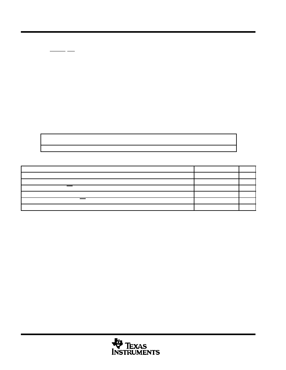
FUNCTION/TRUTH TABLE
INPUTS
OUTPUTS
MR∂
VDD>VIT
RESET
RESET#
L
0
L
H
L
1
L
H
H
0
L
H
H
1
H
L
∂ TPS3820/3/5/8
# TPS3824/5
functional block diagram
_
+
Watchdog
Timer Logic
Reset
Logic
Reset
Reset
MR
WDI
Transition
Detector
52 k
40 k
Vref
VDD
TPS3824/5
TPS3820/3/5/8
timing diagram
undefined
undefined
td
td
tt(out)
td
VDD
VIT
1.1 V
RESET
WDI
TPS3820 xx, TPS3823 xx, TPS3824 xx, TPS3825 xx, TPS3828 xx
PROCESSOR SUPERVISORY CIRCUITS
SLVS165E ≠ APRIL 1998 ≠ REVISED DECEMBER 2002
4
POST OFFICE BOX 655303
∑
DALLAS, TEXAS 75265
absolute maximum ratings over operating free-air temperature range (unless otherwise noted)
Supply voltage, V
DD
(see Note 1)
6 V
. . . . . . . . . . . . . . . . . . . . . . . . . . . . . . . . . . . . . . . . . . . . . . . . . . . . . . . . . . . . .
RESET, RESET, MR, WDI (see Note 1)
≠0.3 V to (V
DD
+ 0.3 V)
. . . . . . . . . . . . . . . . . . . . . . . . . . . . . . . . . . . . . .
Maximum low output current, I
OL
5
mA
. . . . . . . . . . . . . . . . . . . . . . . . . . . . . . . . . . . . . . . . . . . . . . . . . . . . . . . . . . .
Maximum high output current, I
OH
≠5 mA
. . . . . . . . . . . . . . . . . . . . . . . . . . . . . . . . . . . . . . . . . . . . . . . . . . . . . . . . .
Input clamp current range, I
IK
(V
I
< 0 or V
I
> V
DD
)
±
10 mA
. . . . . . . . . . . . . . . . . . . . . . . . . . . . . . . . . . . . . . . . . .
Output clamp current range, I
OK
(V
O
< 0 or V
O
> V
DD
)
±
10 mA
. . . . . . . . . . . . . . . . . . . . . . . . . . . . . . . . . . . . . .
Continuous total power dissipation
See Dissipation Rating Table
. . . . . . . . . . . . . . . . . . . . . . . . . . . . . . . . . . . . .
Operating free-air temperature range, T
A
≠40
∞
C to 85
∞
C
. . . . . . . . . . . . . . . . . . . . . . . . . . . . . . . . . . . . . . . . . . . .
Storage temperature range, T
stg
≠65
∞
C to 150
∞
C
. . . . . . . . . . . . . . . . . . . . . . . . . . . . . . . . . . . . . . . . . . . . . . . . . . .
Soldering temperature
260
∞
C
. . . . . . . . . . . . . . . . . . . . . . . . . . . . . . . . . . . . . . . . . . . . . . . . . . . . . . . . . . . . . . . . . . . .
Stresses beyond those listed under "absolute maximum ratings" may cause permanent damage to the device. These are stress ratings only, and
functional operation of the device at these or any other conditions beyond those indicated under "recommended operating conditions" is not
implied. Exposure to absolute-maximum-rated conditions for extended periods may affect device reliability.
NOTE 1: All voltage values are with respect to GND.
DISSIPATION RATING TABLE
PACKAGE
TA
25
∞
C
POWER RATING
OPERATING FACTOR
ABOVE TA = 25
∞
C
TA = 70
∞
C
POWER RATING
TA = 85
∞
C
POWER RATING
DBV
437 mW
3.5 mW/
∞
C
280 mW
227 mW
recommended operating conditions
MIN
MAX
UNIT
Supply voltage, VDD
1.1
5.5
V
Input voltage, VI
0
VDD + 0.3
V
High-level input voltage at MR and WDI, VIH
0.7
◊
VDD
V
Low-level input voltage, VIL
0.3
◊
VDD
V
Input transition rise and fall rate at MR or WDI,
t/
V
100
ns/V
Operating free-air temperature range, TA
≠40
85
∞
C

TPS3820 xx, TPS3823 xx, TPS3824 xx, TPS3825 xx, TPS3828 xx
PROCESSOR SUPERVISORY CIRCUITS
SLVS165E ≠ APRIL 1998 ≠ REVISED DECEMBER 2002
5
POST OFFICE BOX 655303
∑
DALLAS, TEXAS 75265
electrical characteristics over recommended operating free-air temperature range (unless
otherwise noted)
PARAMETER
TEST CONDITIONS
MIN
TYP
MAX
UNIT
TPS382x-25
VDD = VIT≠ + 0.2 V
IOH = ≠20
µ
A
0 8
V
RESET
TPS382x-30
TPS382x-33
VDD = VIT≠ + 0.2 V
IOH = ≠30
µ
A
0.8
◊
VDD
V
TPS382x-50
VDD = VIT≠ + 0.2 V
IOH = ≠120
µ
A
VDD ≠ 1.5 V
VOH
High-level output voltage
TPS3824-25
TPS3825-25
VDD
1.8 V, IOH = ≠100
µ
A
RESET
TPS3824-30
TPS3825-30
0 8
◊
V
V
RESET
TPS3824-33
TPS3825-33
VDD
1.8 V, IOH = ≠150
µ
A
0.8
◊
VDD
V
TPS3824-50
TPS3825-50
TPS3824-25
TPS3825-25
VDD = VIT≠ + 0.2 V
IOL = 1 mA
RESET
TPS3824-30
TPS3825-30
VDD = VIT≠ + 0.2 V
0 4
V
RESET
TPS3824-33
TPS3825-33
VDD = VIT≠ + 0.2 V
IOL = 1.2 mA
0.4
V
VOL
Low-level output voltage
TPS3824-50
TPS3825-50
VDD = VIT≠ + 0.2 V
IOL = 3 mA
TPS382x-25
VDD = VIT≠ ≠ 0.2 V
IOL = 1 mA
RESET
TPS382x-30
VDD = VIT≠ ≠0.2 V
0 4
V
RESET
TPS382x-33
VDD = VIT≠ 0.2 V
IOL = 1.2 mA
0.4
V
TPS382x-50
VDD = VIT≠ ≠ 0.2 V
IOL = 3 mA
Power-up reset voltage (see Note 2)
VDD
1.1 V, IOL = 20
µ
A
0.4
V
TPS382x-25
2.21
2.25
2.30
TPS382x-30
T
0
∞
C
85
∞
C
2.59
2.63
2.69
V
TPS382x-33
TA = 0
∞
C ≠ 85
∞
C
2.88
2.93
3
V
V
Negative-going input threshold
TPS382x-50
4.49
4.55
4.64
VIT≠
Negative going in ut threshold
voltage (see Note 3)
TPS382x-25
2.20
2.25
2.30
g
TPS382x-30
T
40
∞
C
85
∞
C
2.57
2.63
2.69
V
TPS382x-33
TA = ≠40
∞
C ≠ 85
∞
C
2.86
2.93
3
V
TPS382x-50
4.46
4.55
4.64
TPS382x-25
V
H steresis at V
inp t
TPS382x-30
30
mV
Vhys
Hysteresis at VDD input
TPS382x-33
30
mV
TPS382x-50
50
NOTES:
2. The lowest supply voltage at which RESET becomes active. tr, VDD
15
µ
s/V
3. To ensure best stability of the threshold voltage, a bypass capacitor (ceramic, 0.1
µ
F) should be placed near the supply terminals.