 | –≠–ª–µ–∫—Ç—Ä–æ–Ω–Ω—ã–π –∫–æ–º–ø–æ–Ω–µ–Ω—Ç: TPS60231 | –°–∫–∞—á–∞—Ç—å:  PDF PDF  ZIP ZIP |

www.ti.com
FEATURES
DESCRIPTION
APPLICATIONS
VIN
C1+
C1-
C2+
C2-
EN1
EN2
GND
PGND
VOUT
D1
D2
D3
ISET
0.47
m
F
0.47
m
F
1
m
F
1
m
F
VIN = 2.7 V
to 6.5 V
TPS60231
SLVS544 ≠ OCTOBER 2004
WHITE LED CHARGE PUMP CURRENT SOURCE
WITH PWM BRIGHTNESS CONTROL
∑
Regulated Output Current With 0.4%
The TPS60231 charge pump is optimized for white
Matching
LED supplies in color display backlight applications.
The device provides a constant current for each LED,
∑
Drives up to 3 LEDs at 25 mA Each
which the initial value can be set by an external
∑
LED Brightness Control Through PWM
resistor. The supply voltage ranges from 2.7 V to
Control Signal
6.5 V and is ideally suited for all applications powered
∑
High Efficiency by Fractional Conversion
by a single LI-Ion battery cell or three to four NiCd,
With 1x and 1.5x Modes
NiMH, or alkaline battery cells. Over an input voltage
range from 3.1 V to 6.5 V, the device provides a high
∑
1 MHz Switching Frequency
output current of up to 25 mA per LED with a total of
∑
2.7 V to 6.5 V Operating Input Voltage Range
75 mA. High efficiency is achieved by utilizing a
∑
Internal Softstart Limits Inrush Current
1x/1.5x fractional conversion technique in combi-
nation with very low dropout current sources. In
∑
Low Input Ripple and Low EMI
addition, the current controlled charge pump ensures
∑
Overcurrent and Overtemperature Protected
low input current ripple and EMI. Only two external
∑
Undervoltage Lockout With Hysteresis
1 µF and two 0.47 µF capacitors are required to build
a complete small and low cost power supply solution.
∑
Ultra-Small 3mm x 3mm QFN Package
To reduce board space to a minimum, the device
switches at 1 MHz operating frequency and is avail-
able in a small 16-pin QFN (RGT) package.
∑
White LED Backlight for Color Displays in
Cellular Phones, Smart Phones, PDAs,
Handheld PCs, Digital Cameras, and
Camcorders
∑
Keypad Backlight
Please be aware that an important notice concerning availability, standard warranty, and use in critical applications of Texas
Instruments semiconductor products and disclaimers thereto appears at the end of this data sheet.
PRODUCTION DATA information is current as of publication date.
Copyright © 2004, Texas Instruments Incorporated
Products conform to specifications per the terms of the Texas
Instruments standard warranty. Production processing does not
necessarily include testing of all parameters.
www.ti.com
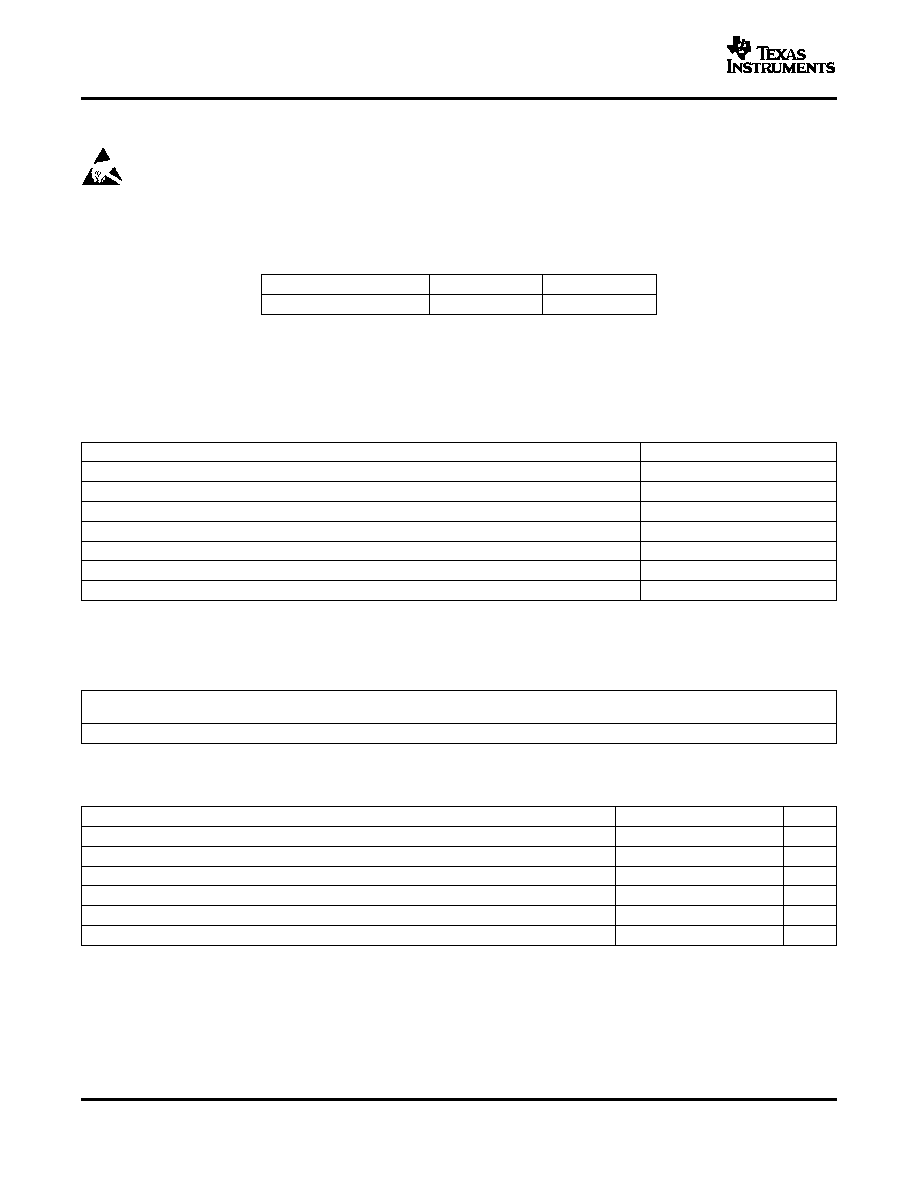
ABSOLUTE MAXIMUM RATINGS
DISSIPATION RATINGS
(1)
RECOMMENDED OPERATING CONDITIONS
TPS60231
SLVS544 ≠ OCTOBER 2004
This integrated circuit can be damaged by ESD. Texas Instruments recommends that all integrated
circuits be handled with appropriate precautions. Failure to observe proper handling and installation
procedures can cause damage.
ESD damage can range from subtle performance degradation to complete device failure. Precision
integrated circuits may be more susceptible to damage because very small parametric changes could
cause the device not to meet its published specifications.
ORDERING INFORMATION
PACKAGED DEVICE
(1) (2)
PACKAGE
MARKING
TPS60231RGTR
QFN
BKH
(1)
T indicates shipment in tape and reel on a mini reel with 250 units
per reel.
(2)
R indicates shipment in tape and reel with 3000 units per reel.
over operating free-air temperature range (unless otherwise noted)
(1)
UNIT
V
I
Supply voltage
≠0.3 V to 7 V
Voltage at EN1, EN2, VOUT, ISET
≠0.3 V to V
I
Output current at VOUT
150 mA
T
J
Maximum junction temperature
150
∞
C
T
A
Operating free-air temperature
≠40
∞
C to 85
∞
C
T
st
Storage temperature
≠65
∞
C to 150
∞
C
Lead temperature 1,6 mm (1/16 inch) from case for 10 seconds
300
∞
C
(1)
Stresses beyond those listed under "absolute maximum ratings" may cause permanent damage to the device. These are stress ratings
only, and functional operation of the device at these or any other conditions beyond those indicated under "recommended operating
conditions" is not implied. Exposure to absolute-maximum-rated conditions for extended periods may affect device reliability.
T
A
25
∞
C
DERATING FACTOR
T
A
= 70
∞
C
T
A
= 85
∞
C
PACKAGE
POWER RATING
ABOVE T
A
= 25
∞
C
POWER RATING
POWER RATING
16-Pin QFN (RGT)
1.9 W
20 mW/
∞
C
1 W
760 mW
(1)
The thermal resistance junction to ambient of the QFN package is 52
∞
C/W.
MIN
TYP
MAX
UNIT
Supply voltage at VIN
2.7
6.5
V
Maximum output current at VOUT
75
mA
C
i
Input capacitor
1
µF
C
o
Output capacitor
0.47
1
µF
Flying capacitor, C1, C2
0.22
0.47
µF
Operating junction temperature
-40
125
∞
C
2

www.ti.com
ELECTRICAL CHARACTERISTICS
TPS60231
SLVS544 ≠ OCTOBER 2004
V
I
= 3.6 V, EN1 = EN2 = V
I
, T
A
= -40
∞
C to 85
∞
C (unless otherwise noted)
PARAMETER
TEST CONDITIONS
MIN
TYP
MAX
UNIT
SUPPLY VOLTAGE AND CURRENT
V
I
Input voltage range
I
O
= 0 mA to 75 mA
2.7
6.5
V
V
I
= 4.2 V, x1-mode, EN1 = EN2 = 1, ISET = 20 µA
200
µA
I
Q
Operating quiescent current
I
O
= 0 mA, x1.5-mode
2.1
mA
I
SD
Shutdown current
EN2 = EN1 = GND
0.1
1
µA
CHARGE PUMP STAGE
V
OUT
Overvoltage limit
LED1 unconnected, V
I
= 4.2 V
5.5
V
Startup time
C
O
= 1 µF, I
DX
0.9 I
DX
, set
375
µs
Softstart duration
160
µs
f
Switching frequency
0.75
1
1.25
MHz
Efficiency
V
I
= 3.7 V, I
LED
= 15 mA each, V
DX
= 3.1 V
83%
Shutdown temperature
Temperature rising
160
∞
C
Shutdown temperature hysteresis
20
∞
C
Input current limit
EN2 = EN1 = 1, ISET = 100 µA
350
mA
CURRENT SINKS
Recommended maximum current per cur-
3.2 V
V
I
6.5 V
25
mA
I
Dx
rent sink
Current into each current sink when ISET
50
mA
I
Dx
3.0 V
V
I
6.5 V, ISET shorted to GND
is shorted to GND
Current matching between any two outputs
V
Dx
= 3.1 V, T
A
= 25
∞
C
≠2% 0.4%
2%
3.2 V
V
I
6.5 V, V
Dx
= 3.1 V, EN1 = EN2 = 1,
±
3%
Line regulation
ISET = 80 µA
EN2 = 0, EN1 = 1
200
V
ISET
Reference voltage for current set
EN2 = 1, EN1 = 0
400
mV
EN2 = 1, EN1 = 1
580
600
620
Iset
Recommended ISET pin current range
4
130
µA
K
I
Dx
to ISET current ratio
EN2 = EN1 = 1, ISET = 80 µA
230
260
280
EN2 = 0, EN1 = 1
200
V
source
Voltage at Dx to GND
EN2 = 1, EN1 = 0
300
mV
EN2 = 1, EN1 = 1
400
ENABLE 1, ENABLE 2
V
IH
EN1, EN2 high level input voltage
1.3
V
V
IL
EN1, EN2 low level input voltage
0.3
V
EN1, EN2 trip point hysteresis
50
mV
I
IKG
EN2 input leakage current
EN1, EN2 = GND or EN2 = V
I
, V
I
= 6.5 V
0.01
1
µA
I
IKG
EN1 input leakage current
EN1 = V
I
, V
I
= 4.2 V
11
15
µA
V
(UVLO)
Undervoltage lockout threshold
Input voltage falling
2.1
V
Undervoltage lockout hysteresis
50
mV
Frequency range at PWM
0
50
kHz
Recommended ON-time for PWM signal
2.5
µs
Delay time when EN1 = EN2 go to GND after which
Shutdown delay time
0.5
0.85
1.5
ms
the TPS60231 shuts down completely
3

www.ti.com
PIN ASSIGNMENT
C2-
C1-
C1+
C2+
PGND
VIN
EN1
D2
D1
VOUT
ISET
GND
NC
NC
D3
3
1
2
7
5
6
8
12
11
10
9
15
13
14
16
EN2
4
QFN PACKAGE
(TOP VIEW)
TPS60231
SLVS544 ≠ OCTOBER 2004
Terminal Functions
TERMINAL
I/O
DESCRIPTION
NAME
NO.
C1+
10
≠
Connect to the flying capacitor C1
C1≠
11
≠
Connect to the flying capacitor C1
C2+
9
≠
Connect to the flying capacitor C2
C2≠
12
≠
Connect to the flying capacitor C2
D1-D3
6-4
I
Current sink input. Connect the cathode of the white LEDs to these inputs.
Enable input. A logic high enables the converter, logic low forces the device into shutdown mode reducing
EN1
15
I
the supply current to less than 1 µA if EN2 is tied to GND.
An applied PWM signal reduces the LED current as a function of the duty cycle of the PWM signal. EN1 and
EN2 can be tied together for PWM dimming between 0 mA and the maximum set with ISET. EN1 and EN2
EN2
16
I
can also be used for digital dimming with 4 steps from 0 mA to the maximum current set with ISET. See the
application section for more details.
GND
14
≠
Analog ground
ISET
1
I
Connect a resistor between this pin and GND to set the maximum current through the LEDs.
NC
2, 3
≠
No internal connection
PGND
7
≠
Power ground
VIN
13
I
Supply voltage input
VOUT
8
0
Connect the output capacitor and the anode of the LEDs to this pin.
Power PAD
≠
≠
Connect with PGND and GND
4

www.ti.com
D3
D2
D1
C1+
C1-
C2+
C2-
EN2
VOUT
ISET
GND
EN1
Control
RSET
VIN
Reference
0.47
m
F
0.47
m
F
1
m
F
Charge
Pump
Current
Sinks
1
m
F
PGND
TPS60231
SLVS544 ≠ OCTOBER 2004
FUNCTIONAL BLOCK DIAGRAM
5