
www.ti.com
FEATURES
DESCRIPTION
APPLICATIONS
3
2
4
5
DBV PACKAGE
(TOP VIEW)
1
SW
GND
FB
V
IN
EN
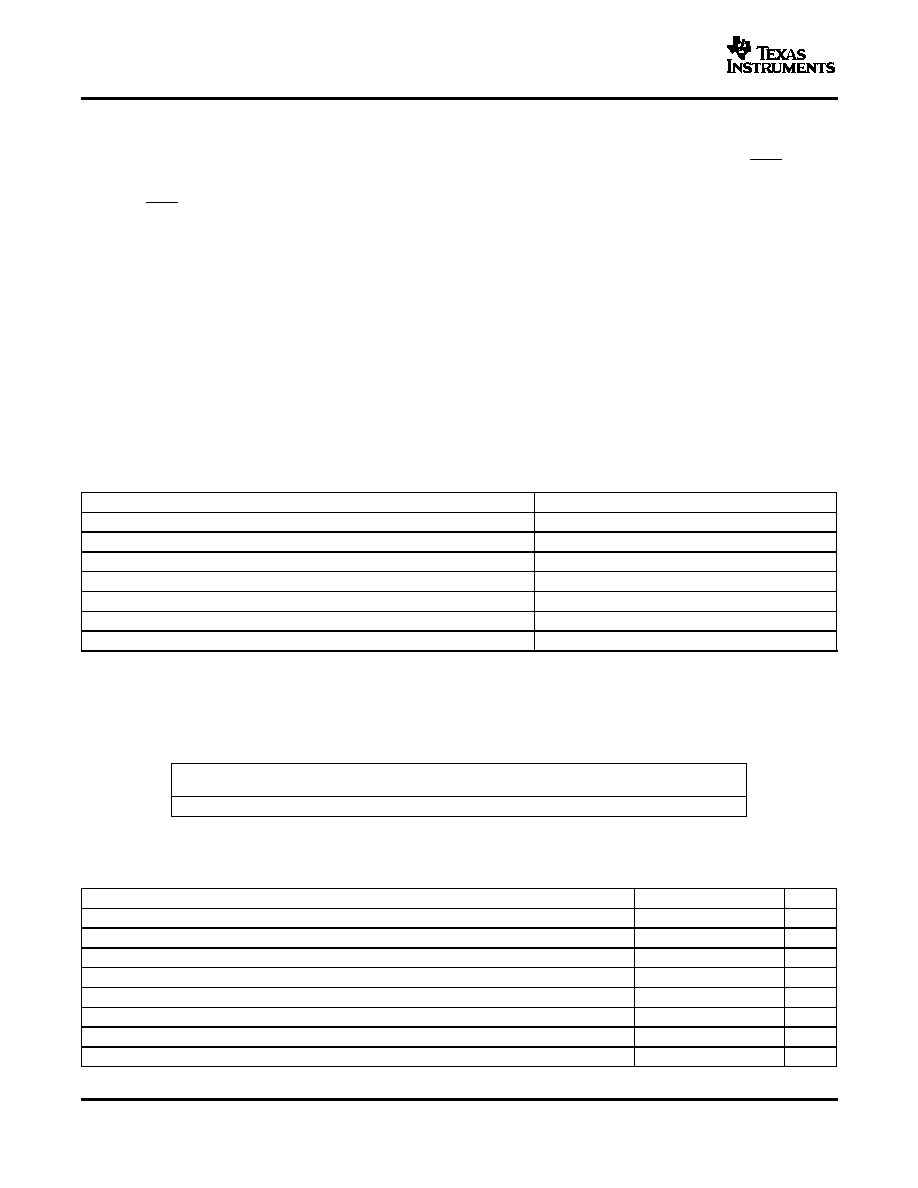
TYPICAL APPLICATION
V
IN
SW
FB
EN
GND
L1
10
µ
H
D1
R1
R2
C
FF
C
O
1
µ
F
V
OUT
V
IN
to 28 V
V
IN
1.8 V to 6.0 V
C
IN
4.7
µ
F
70
72
74
76
78
80
82
84
86
88
90
0.10
1
10
100
V
I
= 5 V
V
I
= 3.6 V
V
I
= 2.4 V
Efficiency - %
EFFICIENCY
vs
OUTPUT CURRENT
I
O
- Output Current - mA
5
4
2
3
1
V
O
= 18 V
TPS61040
TPS61041
SLVS413B ≠ OCTOBER 2002 ≠ REVISED MAY 2004
LOW POWER DC/DC BOOST CONVERTER IN SOT-23 PACKAGE
∑
1.8 V to 6 V Input Voltage Range
The TPS61040/41 is a high-frequency boost con-
verter dedicated for small to medium LCD bias supply
∑
Adjustable Output Voltage Range up to 28 V
and white LED backlight supplies. The device is ideal
∑
400 mA (TPS61040) and 250 mA (TPS61041)
to generate output voltages up to 28 V from a dual
Internal Switch Current
cell NiMH/NiCd or a single cell Li-Ion battery. The
∑
Up to 1 MHz Switching Frequency
part can also be used to generate standard 3.3 V/5 V
to 12 V power conversions.
∑
28 µA Typical No Load Quiescent Current
∑
1 µA Typical Shutdown Current
The TPS61040/41 operates with a switching fre-
quency up to 1 MHz. This allows the use of small
∑
Internal Softstart
external components using ceramic as well as tanta-
∑
Available in a Tiny 5-Pin SOT23 Package
lum output capacitors. Together with the tiny SOT23
package, the TPS61040/41 gives a very small overall
solution size. The TPS61040 has an internal 400 mA
∑
LCD Bias Supply
switch current limit, while the TPS61041 has a 250
mA switch current limit, offering lower output voltage
∑
White-LED Supply for LCD Backlights
ripple and allows the use of a smaller form factor
∑
Digital Still Camera
inductor for lower power applications. The low quiesc-
∑
PDAs, Organizers and Handheld PCs
ent current (typically 28 µA) together with an
∑
Cellular Phones
optimized control scheme, allows device operation at
∑
Internet Audio Player
very high efficiencies over the entire load current
range.
∑
Standard 3.3 V/5 V to 12 V Conversion
Please be aware that an important notice concerning availability, standard warranty, and use in critical applications of Texas
Instruments semiconductor products and disclaimers thereto appears at the end of this data sheet.
PRODUCTION DATA information is current as of publication date.
Copyright © 2002≠2004, Texas Instruments Incorporated
Products conform to specifications per the terms of the Texas
Instruments standard warranty. Production processing does not
necessarily include testing of all parameters.

www.ti.com
+
+
-
RS Latch
Logic
S
R
Gate
Driver
_
Current Limit
Power MOSFET
N-Channel
R
SENSE
Soft
Start
6
µ
s Max
On Time
V
REF
= 1.233 V
Error Comparator
400 ns Min
Off Time
Under Voltage
Lockout
Bias Supply
VIN
FB
EN
GND
SW
TPS61040
TPS61041
SLVS413B ≠ OCTOBER 2002 ≠ REVISED MAY 2004
These devices have limited built-in ESD protection. The leads should be shorted together or the device
placed in conductive foam during storage or handling to prevent electrostatic damage to the MOS gates.
ORDERING INFORMATION
(1)
T
A
SWITCH CURRENT LIMIT
SOT23 PACKAGE
PACKAGE MARKING
400 mA
TPS61040DBV
PHOI
-40 to 85
∞
C
250 mA
TPS61041DBV
PHPI
(1)
The DBV package is available in tape & reel. Add R suffix (DBVR) to order quantities of 3000 parts.
FUNCTIONAL BLOCK DIAGRAM
2

www.ti.com
DETAILED DESCRIPTION
OPERATION
PEAK CURRENT CONTROL
I
peak(typ)
+
I
LIM
)
Vin
L
100 ns
I
peak(typ)
+
400 mA
)
Vin
L
100 ns for the TPS61040
I
peak(typ)
+
250 mA
)
Vin
L
100 ns for the TPS61041
(1)
SOFTSTART
TPS61040
TPS61041
SLVS413B ≠ OCTOBER 2002 ≠ REVISED MAY 2004
Terminal Functions
TERMINAL
I/O
DESCRIPTION
NAME
NO.
SW
1
I
Connect the inductor and the Schottky diode to this pin. This is the switch pin and is connected to the drain of the
internal power MOSFET.
GND
2
Ground
FB
3
I
This is the feedback pin of the device. Connect this pin to the external voltage divider to program the desired output
voltage.
EN
4
I
This is the enable pin of the device. Pulling this pin to ground forces the device into shutdown mode reducing the
supply current to less than 1 µA. This pin should not be left floating and needs to be terminated.
VIN
5
I
Supply voltage pin
The TPS61040/41 operates with an input voltage range of 1.8 V to 6 V and can generate output voltages up to
28 V. The device operates in a pulse frequency modulation (PFM) scheme with constant peak current control.
This control scheme maintains high efficiency over the entire load current range, and with a switching frequency
up to 1 MHz, the device enables the use of very small external components.
The converter monitors the output voltage, and as soon as the feedback voltage falls below the reference voltage
of typically 1.233 V, the internal switch turns on and the current ramps up. The switch turns off as soon as the
inductor current reaches the internally set peak current of typically 400 mA (TPS61040) or 250 mA (TPS61041).
Refer to the section peak current control for more information. The second criteria that turns off the switch is the
maximum on-time of 6 µs (typical). This is just to limit the maximum on-time of the converter to cover for extreme
conditions. As the switch is turned off the external Schottky diode is forward biased delivering the current to the
output. The switch remains off for a minimum of 400 ns (typical), or until the feedback voltage drops below the
reference voltage again. Using this PFM peak current control scheme the converter operates in discontinuous
conduction mode (DCM) where the switching frequency depends on the output current, which results in very high
efficiency over the entire load current range. This regulation scheme is inherently stable, allowing a wider
selection range for the inductor and output capacitor.
The internal switch turns on until the inductor current reaches the typical dc current limit (I
LIM
) of 400 mA
(TPS61040) or 250 mA (TPS61042). Due to the internal propagation delay of typical 100 ns, theactualcurrent
exceeds the dc current limit threshold by a small amount. The typical peak current limit can be calculated:
The higher the input voltage and the lower the inductor value, the greater the peak.
By selecting the TPS61040 or TPS61041, it is possible to tailor the design to the specific application current limit
requirements. A lower current limit supports applications requiring lower output power and allows the use of an
inductor with a lower current rating and a smaller form factor. A lower current limit usually has a lower output
voltage ripple as well.
All inductive step-up converters exhibit high inrush current during start-up if no special precaution is made. This
can cause voltage drops at the input rail during start up and may result in an unwanted or early system shut
down.
3
www.ti.com
The TPS61040/41 limits this inrush current by increasing the current limit in two steps starting from
I
LIM
4
for 256
cycles to
I
LIM
2
for the next 256 cycles, and then full current limit (refer to Figure 14).
ENABLE
UNDERVOLTAGE LOCKOUT
ABSOLUTE MAXIMUM RATINGS
DISSIPATION RATING TABLE
(1)
RECOMMENDED OPERATING CONDITIONS
TPS61040
TPS61041
SLVS413B ≠ OCTOBER 2002 ≠ REVISED MAY 2004
DETAILED DESCRIPTION (continued)
Pulling the enable (EN) to ground shuts down the device reducing the shutdown current to 1 µA (typical). Since
there is a conductive path from the input to the output through the inductor and Schottky diode, the output
voltage is equal to the input voltage during shutdown. The enable pin needs to be terminated and should not be
left floating. Using a small external transistor disconnects the input from the output during shutdown as shown in
Figure 18.
An undervoltage lockout prevents misoperation of the device at input voltages below typical 1.5 V.When the input
voltage is below the undervoltage threshold the main switch is turned off.
over operating free-air temperature (unless otherwise noted)
(1)
UNIT
Supply voltages on pin VIN
(2)
-0.3 V to 7 V
Voltages on pins EN, FB
(2)
-0.3 V to V
IN
+ 0.3 V
Switch voltage on pin SW
(2)
30 V
Continuous power dissipation
See Dissipation Rating Table
T
J
Operating junction temperature
-40
∞
C to 150
∞
C
T
Stg
Storage temperature
-65
∞
C to 150
∞
C
Lead temperature (soldering 10 seconds)
260
∞
C
(1)
Stresses beyond those listed under absolute maximum ratings may cause permanent damage to the device. These are stress ratings
only, and functional operation of the device at these or any other conditions beyond those indicated under recommended operating
conditions is not implied. Exposure to absolute-maximum-rated conditions for extended periods may affect device reliability.
(2)
All voltage values are with respect to network ground terminal.
T
A
25
∞
C
DERATING FACTOR
T
A
= 70
∞
C
T
A
= 85
∞
C
PACKAGE
POWER RATING
ABOVE T
A
= 25
∞
C
POWER RATING
POWER RATING
DBV
357 mW
3.5 mW/
∞
C
192 mW
140 mW
(1)
The thermal resistance junction to ambient of the 5-pin SOT23 is 250
∞
C/W.
MIN
TYP
MAX
UNIT
Vin
Input voltage range
1.8
6
V
V
OUT
Output voltage range
28
V
L
Inductor
(1)
2.2
10
µH
f
Switching frequency
(1)
1
MHz
C
in
Input capacitor
(1)
4.7
µF
C
OUT
Output capacitor
(1)
1
µF
T
A
Operating ambient temperature
-40
85
∞
C
T
J
Operating junction temperature
-40
125
∞
C
(1)
Refer to application section for further information
4

www.ti.com
ELECTRICAL CHARACTERISTICS
TPS61040
TPS61041
SLVS413B ≠ OCTOBER 2002 ≠ REVISED MAY 2004
Vin = 2.4 V, EN = VIN, T
A
= -40
∞
C to 85
∞
C, typical values are at T
A
= 25
∞
C (unless otherwise noted)
PARAMETER
TEST CONDITIONS
MIN
TYP
MAX
UNIT
SUPPLY CURRENT
Vin
Input voltage range
1.8
6
V
I
Q
Operating quiescent current
I
OUT
= 0 mA, not switching, V
FB
= 1.3 V
28
50
µA
I
SD
Shutdown current
EN=GND
0.1
1
µA
V
UVLO
Under-voltage lockout threshold
1.5
1.7
V
ENABLE
V
IH
EN high level input voltage
1.3
V
V
IL
EN low level input voltage
0.4
V
I
I
EN input leakage current
EN = GND or VIN
0.1
1
µA
POWER SWITCH AND CURRENT LIMIT
Vsw
Maximum switch voltage
30
V
t
off
Minimum off time
250
400
550
ns
t
on
Maximum on time
4
6
7.5
µs
R
DS(ON)
MOSFET on-resistance
Vin = 2.4 V; Isw = 200 mA; TPS61040
600
1000
m
R
DS(ON)
MOSFET on-resistance
Vin = 2.4 V; Isw = 200 mA; TPS61041
750
1250
m
MOSFET leakage current
V
sw
= 28 V
1
10
µA
I
LIM
MOSFET current limit
TPS61040
350
400
450
mA
I
LIM
MOSFET current limit
TPS61041
215
250
285
mA
OUTPUT
V
OUT
Adjustable output voltage range
Vin
28
V
V
ref
Internal voltage reference
1.233
V
I
FB
Feedback input bias current
V
FB
= 1.3 V
1
µA
V
FB
Feedback trip point voltage
1.8 V
Vin
6.0 V
1.208
1.233
1.258
V
1.8 V
Vin
6.0 V; Vout = 18 V; Iload = 10 mA
Line regulation
(1)
0.05
%/V
Cff = not connected
Load regulation
(1)
Vin = 2.4 V; Vout = 18 V; 0 mA
Iout
30 mA
0.15
%/mA
(1)
The line and load regulation depend on the external component selection. Refer to the application section for further information.
5