TPS62000, TPS62001, TPS62002, TPS62003
TPS62004, TPS62005, TPS62006, TPS62007, TPS62008
HIGH EFFICIENCY STEP DOWN LOW POWER DC DC CONVERTER
SLVS294C - SEPTEMBER 2000 - REVISED SEPTEMBER 2003
1
POST OFFICE BOX 655303
∑
DALLAS, TEXAS 75265
FEATURES
D
High-Efficiency Synchronous Step-Down
Converter With Greater Than 95%
Efficiency
D
2 V to 5.5 V Operating Input Voltage Range
D
Adjustable Output Voltage Range From
0.8 V to V
I
D
Fixed Output Voltage Options Available in
0.9 V, 1 V, 1.2 V, 1.5 V, 1.8 V, 1.9 V, 2.5 V, and
3.3 V
D
Synchronizable to External Clock Signal up
to 1 MHz
D
Up to 600 mA Output Current
D
Pin-Programmable Current Limit
D
High Efficiency Over a Wide Load Current
Range in Power Save Mode
D
100% Maximum Duty Cycle for Lowest
Dropout
D
Low-Noise Operation Antiringing Switch
and PFM/PWM Operation Mode
D
Internal Softstart
D
50-
µ
A Quiescent Current (TYP)
D
Available in the 10-Pin Microsmall Outline
Package (MSOP)
D
Evaluation Module Available
D
Available in a Ultra-Small, 12-Pin
NanoStar
E
(Wafer Chip-Scale) Package
APPLICATIONS
D
Low-Power CPUs and DSPs
D
Cellular Phones
D
Organizers, PDAs, and Handheld PCs
D
MP-3 Portable Audio Players
D
Digital Cameras
D
USB-Based DSL Modems and Other
Network Interface Cards
description
The TPS6200x devices are a family of low-noise synchronous step-down dc-dc converters that are ideally
suited for systems powered from a 1-cell Li-ion battery or from a 2- to 3-cell NiCd, NiMH, or alkaline battery. The
TPS6200x operates typically down to an input voltage of 1.8 V, with a specified minimum input voltage of 2 V.
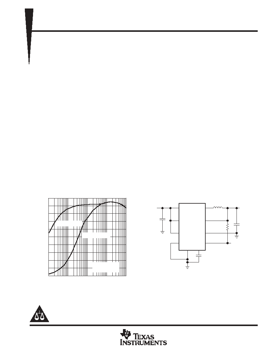
0
10
20
30
40
50
60
70
80
90
100
0.1
1
10
100
1000
Efficiency - %
EFFICIENCY
vs
LOAD CURRENT
IO - Load Current - mA
VI = 3.6 V,
VO = 2.5 V
Figure 1
V
IN
1
8
6
7
3
2
9
5
10
4
10
µ
H
EN
ILIM
SYNC
GND
FC
PG
PGND
FB
L
TPS6200x
10
µ
F
V
O
= 0.8 V
to V
I
PG
0.1
µ
F
10
µ
F
V
I
= 2 V
to 5.5 V
With VO
1.8 V; Co = 10
µ
F, VO <1.8 V; Co = 47
µ
F
Figure 2. Typical Application Circuit for Fixed
Output Voltage Option
SYNC = Low
SYNC = High
Copyright
2002-2003, Texas Instruments Incorporated
PRODUCTION DATA information is current as of publication date.
Products conform to specifications per the terms of Texas Instruments
standard warranty. Production processing does not necessarily include
testing of all parameters.
Please be aware that an important notice concerning availability, standard warranty, and use in critical applications of
Texas Instruments semiconductor products and disclaimers thereto appears at the end of this data sheet.
TPS62000, TPS62001, TPS62002, TPS62003
TPS62004, TPS62005, TPS62006, TPS62007, TPS62008
HIGH EFFICIENCY STEP DOWN LOW POWER DC DC CONVERTER
SLVS294C - SEPTEMBER 2000 - REVISED SEPTEMBER 2003
2
POST OFFICE BOX 655303
∑
DALLAS, TEXAS 75265
description (continued)
The TPS6200x is a synchronous current-mode PWM converter with integrated N- and P-channel power
MOSFET switches. Synchronous rectification is used to increase efficiency and to reduce external component
count. To achieve the highest efficiency over a wide load current range, the converter enters a power-saving
pulse-frequency modulation (PFM) mode at light load currents. Operating frequency is typically 750 kHz,
allowing the use of small inductor and capacitor values. The device can be synchronized to an external clock
signal in the range of 500 kHz to 1 MHz. For low-noise operation, the converter can be operated in the PWM
mode and the internal antiringing switch reduces noise and EMI. In the shutdown mode, the current
consumption is reduced to less than 1
µ
A. The TPS6200x is available in the 10-pin (DGS) microsmall outline
package (MSOP). The TPS62000 is also available in a 12-pin, 1,85 mm x 1,3 mm NanoStar
chip scale
package (YEG). The devices operate over a free-air temperature range of -40
∞
C to 85
∞
C.
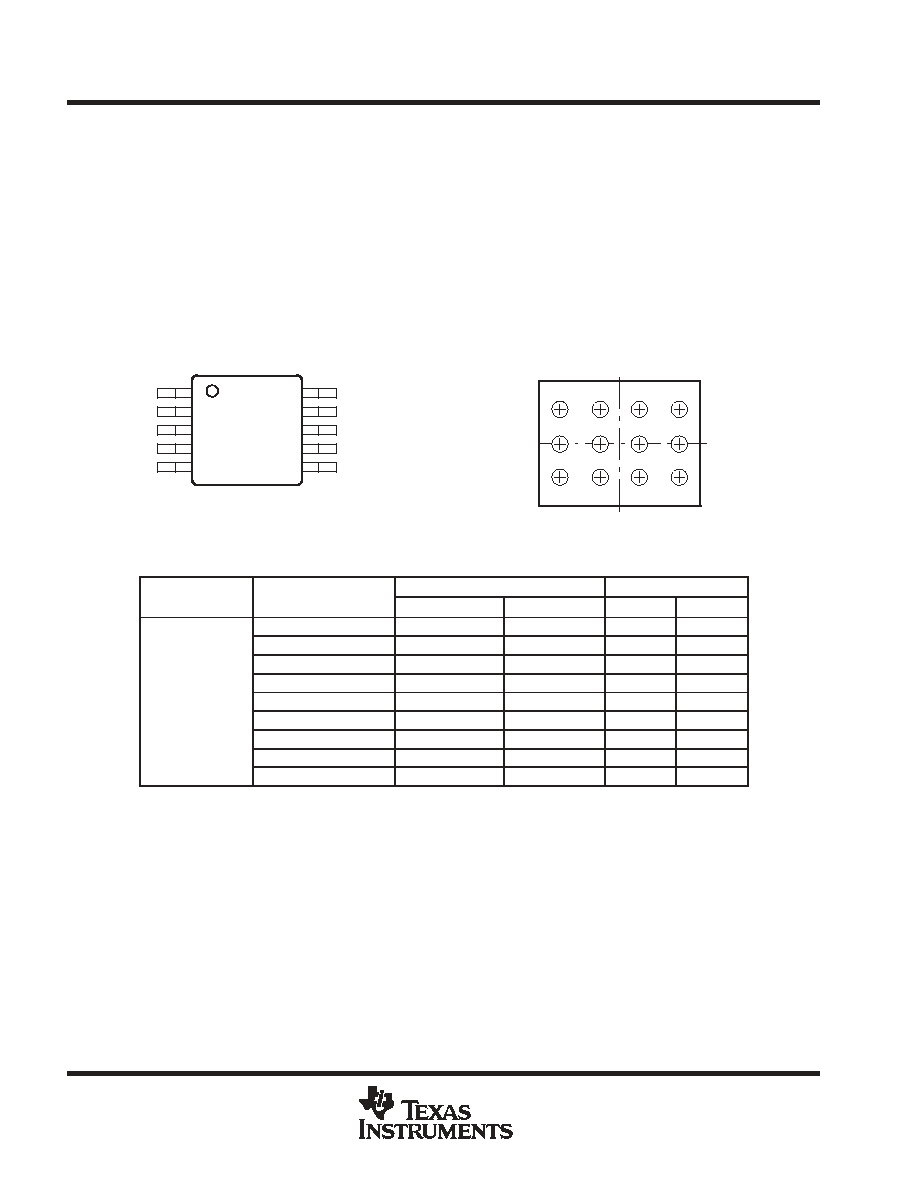
1
2
3
4
5
10
9
8
7
6
MSOP (DGS) PACKAGE
(TOP VIEW)
V
IN
FC
GND
PG
FB
PGND
L
EN
SYNC
ILIM
A
B
C
D
1
2
3
YEG PACKAGE
(BOTTOM VIEW)
AVAILABLE OPTIONS
TA
VOLTAGE OPTIONS
PACKAGE
MARKING
TA
VOLTAGE OPTIONS
MSOP
WCSP
DGS
YEG
Adjustable
TPS62000DGS
TPS62000YEG
AIH
TPS62000
0.9 V
TPS62001DGS
AII
1 V
TPS62002DGS
AIJ
1.2 V
TPS62003DGS
AIK
- 40
∞
C to 85
∞
C
1.5 V
TPS62004DGS
AIL
- 40 C to 85 C
1.8 V
TPS62005DGS
AIM
1.9 V
TPS62008DGS
AJI
2.5 V
TPS62006DGS
AIN
3.3 V
TPS62007DGS
AIO
Without the suffix indicates deliveries in tubes of 80 units.
The YEG package is available taped and reeled. Add R suffix to device type (e.g. TPS62000YEGR) to order
3000 devices per reel. Add T sufix to device type (e.g., TPS62000YEGT) to order 250 devices per reel.
TPS62000, TPS62001, TPS62002, TPS62003
TPS62004, TPS62005, TPS62006, TPS62007, TPS62008
HIGH EFFICIENCY STEP DOWN LOW POWER DC DC CONVERTER
SLVS294C - SEPTEMBER 2000 - REVISED SEPTEMBER 2003
3
POST OFFICE BOX 655303
∑
DALLAS, TEXAS 75265
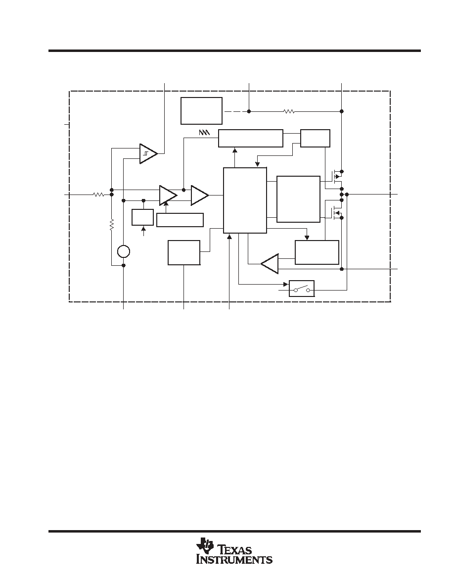
functional block diagram
PFM/PWM
Control Logic
Current Limit
Logic
_
+
Compensation
Soft
Start
Slope Compensation
PFM/PWM
Mode Select
PFM/PWM
Comparator
Error Amplifier
_
+
Current
Sense
Driver
Shoot-Through
Logic
_
+
Undervoltage
Lockout
Bias Supply
10
_
+
Vref = 0.45 V
R2
R1
R1 + R2
1 M
Power Good
Sync
+
Oscillator
_
+
Load Comparator
Current Sense
+
Offset
Antiringing
FB
N-Channel
Power MOSFET
P-Channel
Power MOSFET
L
PGND
EN
FB
PG
FC (See Note B)
VIN
GND
SYNC
ILIM
EN
(See
Note A)
NOTES: A. The adjustable output voltage version does not use the internal feedback resistor divider. The FB pin is directly connected to the
error amplifier.
B. Do not connect the FC pin to an external power source

TPS62000, TPS62001, TPS62002, TPS62003
TPS62004, TPS62005, TPS62006, TPS62007, TPS62008
HIGH EFFICIENCY STEP DOWN LOW POWER DC DC CONVERTER
SLVS294C - SEPTEMBER 2000 - REVISED SEPTEMBER 2003
4
POST OFFICE BOX 655303
∑
DALLAS, TEXAS 75265
Terminal Functions
TERMINAL
NAME
NO.
I/O
DESCRIPTION
NAME
DGS
YEG
I/O
DESCRIPTION
EN
8
B3
I
Enable. A logic high enables the converter, logic low forces the device into shutdown mode reducing the
supply current to less than 1
µ
A.
FB
5
A2
I
Feedback pin for the fixed output voltage option. For the adjustable version an external resistive divider is
connected to FB. The internal voltage divider is disabled for the adjustable version.
FC
2
C1
Supply bypass pin. A 0.1
µ
F coupling capacitor should be connected as close as possible to this pin for good
high frequency input voltage supply filtering.
GND
3
A1
Ground
ILIM
6
A3
I
Switch current limit. Connect ILIM to GND to set the switch current limit to typically 600 mA, or connect this
pin to VIN to set the current limit to typically 1200 mA.
L
9
C2,
C3
I/O
Connect the inductor to this pin. L is the switch pin connected to the drain of the internal power MOSFETS.
PG
4
B1
O
Power good comparator output. This is an open-drain output. A pullup resistor should be connected
between PG and VO. The output goes active high when the output voltage is greater than 92% of the nominal
value.
PGND
10
D2
Power ground. Connect all power grounds to PGND.
SYNC
7
D3
I
Input for synchronization to external clock signal. Synchronizes the converter switching frequency to an
external clock signal with CMOS level:
SYNC = HIGH: Low-noise mode enabled, fixed frequency PWM operation is forced
SYNC = LOW (GND): Power save mode enabled, PFM/PWM mode enabled.
VIN
1
D1
I
Supply voltage input
NC
B2
Not connected
detailed description
operation
The TPS6200x is a step down converter operating in a current mode PFM/PWM scheme with a typical switching
frequency of 750 kHz.
At moderate to heavy loads, the converter operates in the pulse width modulation (PWM) and at light loads the
converter enters a power save mode (pulse frequency modulation) to keep the efficiency high.
In the PWM mode operation, the part operates at a fixed frequency of 750 kHz. At the beginning of each clock
cycle, the high side P-channel MOSFET is turned on. The current in the inductor ramps up and is sensed via
an internal circuit. The high side switch is turned off when the sensed current causes the PFM/PWM comparator
to trip when the output voltage is in regulation or when the inductor current reaches the current limit (set by ILIM).
After a minimum dead time preventing shoot through current, the low side N-channel MOSFET is turned on and
the current ramps down again. As the clock cycle is completed, the low side switch is turned off and the next
clock cycle starts.
In discontinuous conduction mode (DCM), the inductor current ramps to zero before the end of each clock cycle.
In order to increase the efficiency the load comparator turns off the low side MOSFET before the inductor current
becomes negative. This prevents reverse current flowing from the output capacitor through the inductor and
low side MOSFET to ground that would cause additional losses.
As the load current decreases and the peak inductor current does not reach the power save mode threshold
of typically 120 mA for more than 15 clock cycles, the converter enters a pulse frequency modulation (PFM)
mode.

TPS62000, TPS62001, TPS62002, TPS62003
TPS62004, TPS62005, TPS62006, TPS62007, TPS62008
HIGH EFFICIENCY STEP DOWN LOW POWER DC DC CONVERTER
SLVS294C - SEPTEMBER 2000 - REVISED SEPTEMBER 2003
5
POST OFFICE BOX 655303
∑
DALLAS, TEXAS 75265
operation (continued)
In the PFM mode, the converter operates with:
D
Variable frequency
D
Constant peak current that reduces switching losses
D
Quiescent current at a minimum
Thus maintaining the highest efficiency at light load currents. In this mode, the output voltage is monitored with
the error amplifier. As soon as the output voltage falls below the nominal value, the high side switch is turned
on and the inductor current ramps up. When the inductor current reaches the peak current of typical: 150 mA
+ 50 mA/V x (V
I
- V
O
), the high side switch turns off and the low side switch turns on. As the inductor current
ramps down, the low side switch is turned off before the inductor current becomes negative which completes
the cycle. When the output voltage falls below the nominal voltage again, the next cycle is started.
The converter enters the PWM mode again as soon as the output voltage can not be maintained with the typical
peak inductor current in the PFM mode.
The control loop is internally compensated reducing the amount of external components.
The switch current is internally sensed and the maximum current limit can be set to typical 600 mA by connecting
ILIM to ground or to typically 1.2 A connecting ILIM to V
IN
.
100% duty cycle operation
As the input voltage approaches the output voltage and the duty cycle exceeds typical 95%, the converter turns
the P-channel high side switch continuously on. In this mode, the output voltage is equal to the input voltage
minus the voltage drop across the P-channel MOSFET.
synchronization, power save mode and forced PWM mode
If no clock signal is applied, the converter operates with a typical switching frequency of 750 kHz. It is possible
to synchronize the converter to an external clock within a frequency range from 500 kHz to 1000 kHz. The device
automatically detects the rising edge of the first clock and is synchronizes immediately to the external clock.
If the clock signal is stopped, the converter automatically switches back to the internal clock and continues
operation without interruption. The switch over is initiated if no rising edge on the SYNC pin is detected for a
duration of four clock cycles. Therefore, the maximum delay time can be 8
µ
s in case the internal clock has a
minimum frequency of 500 kHz.
In case the device is synchronized to an external clock, the power save mode is disabled and the device stays
in forced PWM mode.
Connecting the SYNC pin to the GND pin enables the power save mode. The converter operates in the PWM
mode at moderate to heavy loads and in the PFM mode during light loads maintaining high efficiency over a
wide load current range.
Connecting the SYNC pin to the V
IN
pin forces the converter to operate permanently in the PWM mode even
at light or no load currents. The advantage is the converter operates with a fixed switching frequency that allows
simple filtering of the switching frequency for noise sensitive applications. In this mode, the efficiency is lower
compared to the power save mode during light loads (see Figure 1).
It is possible to switch from forced PWM mode to the power save mode during operation.
The flexible configuration of the SYNC pin during operation of the device allows efficient power management
by adjusting the operation of the TPS6200x to the specific system requirements.
low noise antiringing switch
An antiringing switch is implemented in order to reduce the EMI radiated from the converter during
discontinuous conduction mode (DCM). In DCM, the inductor current ramps to zero before the end of each
switching period. The internal load comparator turns off the low side switch at that instant thus preventing the