Äîêóìåíòàöèÿ è îïèñàíèÿ www.docs.chipfind.ru
www.ti.com
FEATURES
DESCRIPTION
APPLICATIONS
V
I
GND
EN
SW
FB
C1
4.7
µ
F
L1
10
µ
H
C2
10
µ
F
TPS62202
V
I
2.5 V - 6 V
V
O
1.8 V / 300 mA
1
5
2
3
4
40
45
50
55
60
65
70
75
80
85
90
95
100
0.010
0.100
1
10
100
1000
Efficiency - %
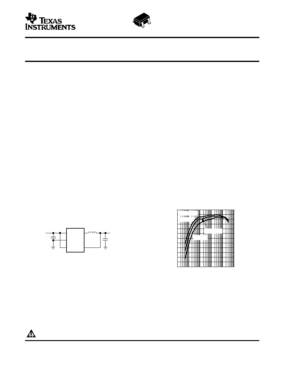
EFFICIENCY
vs
LOAD CURRENT
I
L
-Load Current - mA
V
O
= 1.8 V
V
I
= 2.7 V
V
I
= 3.7 V
V
I
= 5 V
TPS62200, TPS62201
TPS62202, TPS62203, TPS62207
TPS62204, TPS62205, TPS62208
SLVS417D MARCH 2002 REVISED MAY 2004
HIGH-EFFICIENCY, SOT23
STEP-DOWN, DC-DC CONVERTER
·
High Efficiency Synchronous Step-Down
The TPS6220x devices are a family of high-efficiency
Converter With up to 95% Efficiency
synchronous step-down converters ideally suited for
·
2.5 V to 6.0 V Input Voltage Range
portable systems powered by 1-cell Li-Ion or 3-cell
·
Adjustable Output Voltage Range From 0.7 V
NiMH/NiCd batteries. The devices are also suitable to
to V
I
operate from a standard 3.3-V or 5-V voltage rail.
·
Fixed Output Voltage Options Available
With an output voltage range of 6.0 V down to 0.7 V
·
Up to 300 mA Output Current
and up to 300 mA output current, the devices are
ideal to power low voltage DSPs and processors
·
1 MHz Fixed Frequency PWM Operation
used in PDAs, pocket PCs, and smart phones. Under
·
Highest Efficiency Over Wide Load Current
nominal load current, the devices operate with a fixed
Range Due to Power Save Mode
switching frequency of typically 1 MHz. At light load
·
15-µA Typical Quiescent Current
currents, the part enters the power save mode
operation; the switching frequency is reduced and the
·
Soft Start
quiescent current is typically only 15 µA; therefore it
·
100% Duty Cycle Low-Dropout Operation
achieves the highest efficiency over the entire load
·
Dynamic Output-Voltage Positioning
current range. The TPS6220x needs only three small
external components. Together with the tiny SOT23
·
Available in a Tiny 5-Pin SOT23 Package
package, a minimum system solution size can be
achieved. An advanced fast response voltage mode
control scheme achieves superior line and load regu-
·
PDAs and Pocket PC
lation with small ceramic input and output capacitors.
·
Cellular Phones, Smart Phones
·
Low Power DSP Supply
·
Digital Cameras
·
Portable Media Players
·
Portable Equipment
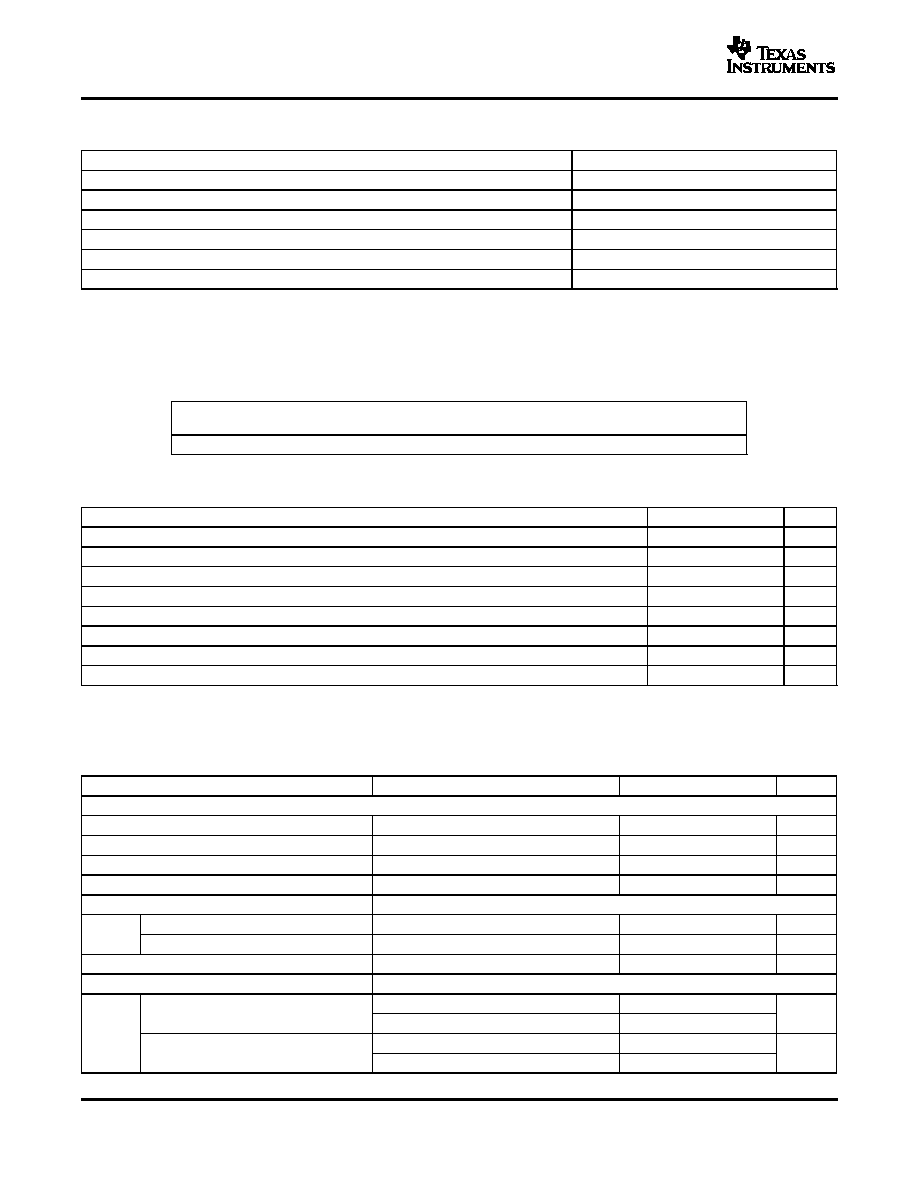
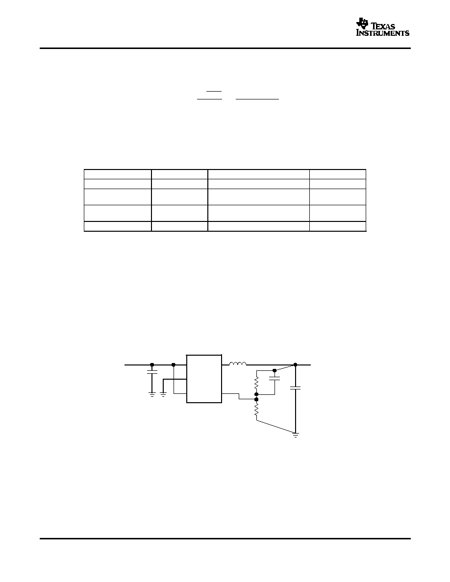
Figure 1. Typical Application
(Fixed Output Voltage Version)
Please be aware that an important notice concerning availability, standard warranty, and use in critical applications of Texas
Instruments semiconductor products and disclaimers thereto appears at the end of this data sheet.
PRODUCTION DATA information is current as of publication date.
Copyright © 20022004, Texas Instruments Incorporated
Products conform to specifications per the terms of the Texas
Instruments standard warranty. Production processing does not
necessarily include testing of all parameters.
www.ti.com
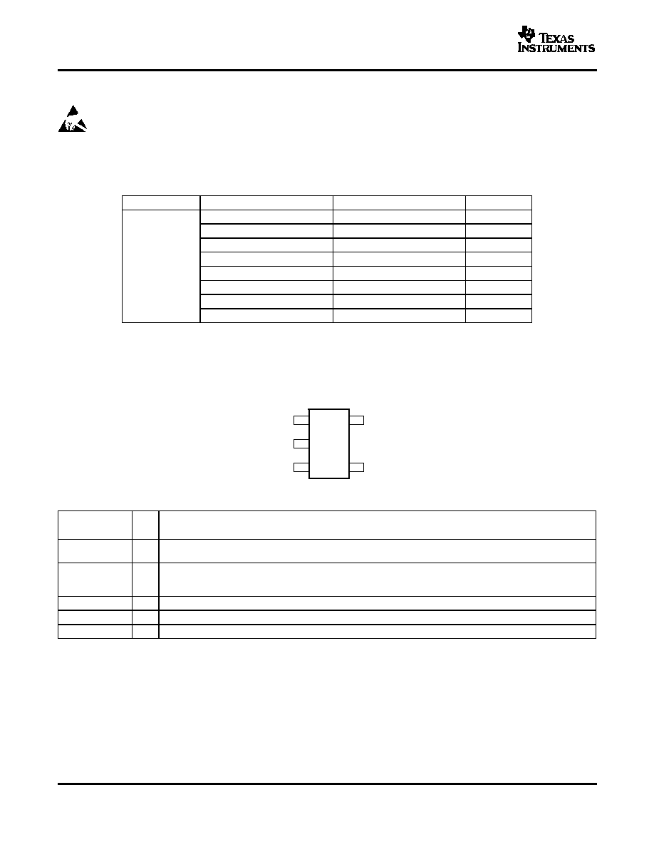
3
2
4
5
DBV PACKAGE
(TOP VIEW)
1
V
I
GND
EN
SW
FB
TPS62200, TPS62201
TPS62202, TPS62203, TPS62207
TPS62204, TPS62205, TPS62208
SLVS417D MARCH 2002 REVISED MAY 2004
This integrated circuit can be damaged by ESD. Texas Instruments recommends that all integrated
circuits be handled with appropriate precautions. Failure to observe proper handling and installation
procedures can cause damage.
ESD damage can range from subtle performance degradation to complete device failure. Precision
integrated circuits may be more susceptible to damage because very small parametric changes could
cause the device not to meet its published specifications.
ORDERING INFORMATION
(1)
T
A
OUTPUT VOLTAGE
SOT23 PACKAGE
SYMBOL
Adjustable
TPS62200DBV
PHKI
1.2 V
TPS62207DBV
PJGI
1.5 V
TPS62201DBV
PHLI
1.6 V
TPS62204DBV
PHSI
-40
°
C to 85
°
C
1.8 V
TPS62202DBV
PHMI
1.875 V
TPS62208DBV
ALW
2.5 V
TPS62205DBV
PHTI
3.3 V
TPS62203DBV
PHNI
(1)
The DBV package is available in tape and reel. Add R suffix (DBVR) to order quantities of 3000 parts.
Add T suffix (DBVT) to order quantities of 250 parts
Terminal Functions
TERMINAL
I/O
DESCRIPTION
NAME
NO.
EN
3
I
This is the enable pin of the device. Pulling this pin to ground forces the device into shutdown mode. Pulling this
pin to Vin enables the device. This pin must not be left floating and must be terminated.
FB
4
I
This is the feedback pin of the device. Connect this pin directly to the output if the fixed output voltage version is
used. For the adjustable version an external resistor divider is connected to this pin. The internal voltage divider
is disabled for the adjustable version.
GND
2
Ground
SW
5
I/O
Connect the inductor to this pin. This pin is the switch pin and is connected to the internal MOSFET switches.
V
I
1
I
Supply voltage pin
2
www.ti.com
_
+
_
+
_
+
_
+
_
+
REF
REF
Load Comparator
Skip Comparator
Current Limit Comparator
P-Channel
Power MOSFET
Driver
Shoot-Through
Logic
Control
Logic
Soft Start
1 MHz
Oscillator
Comparator
S
R
N-Channel
Power MOSFET
Comparator High
Comparator Low
Comparator Low 2
V
(COMP)
Sawtooth
Generator
V
I
Undervoltage
Lockout
Bias Supply
_
+
Comparator High
Comparator Low
Comparator Low 2
Compensation
V
REF
= 0.5 V
R2
See Note
R1
V
I
EN
SW
FB
GND
Gm
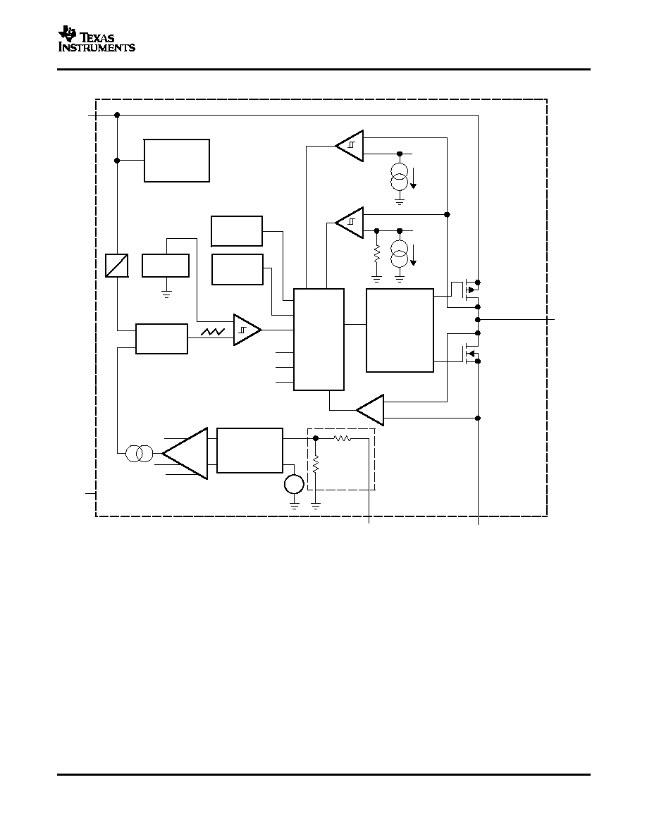
DETAILED DESCRIPTION
OPERATION
TPS62200, TPS62201
TPS62202, TPS62203, TPS62207
TPS62204, TPS62205, TPS62208
SLVS417D MARCH 2002 REVISED MAY 2004
FUNCTIONAL BLOCK DIAGRAM
#IMPLIED.
For the adjustable version (TPS62200) the internal feedback divider is disabled and the FB pin is directly
connected to the internal GM amplifier
The TPS6220x is a synchronous step-down converter operating with typically 1MHz fixed frequency pulse width
modulation (PWM) at moderate to heavy load currents and in power save mode operating with pulse frequency
modulation (PFM) at light load currents.
During PWM operation the converter uses a unique fast response, voltage mode, controller scheme with input
voltage feed forward. This achieves good line and load regulation and allows the use of small ceramic input and
output capacitors. At the beginning of each clock cycle initiated by the clock signal (S), the P-channel MOSFET
switch is turned on, and the inductor current ramps up until the comparator trips and the control logic turns off the
switch. The current limit comparator also turns off the switch in case the current limit of the P-channel switch is
exceeded. Then the N-channel rectifier switch is turned on and the inductor current ramps down. The next cycle
is initiated by the clock signal again turning off the N-channel rectifier and turning on the P-channel switch.
3
www.ti.com
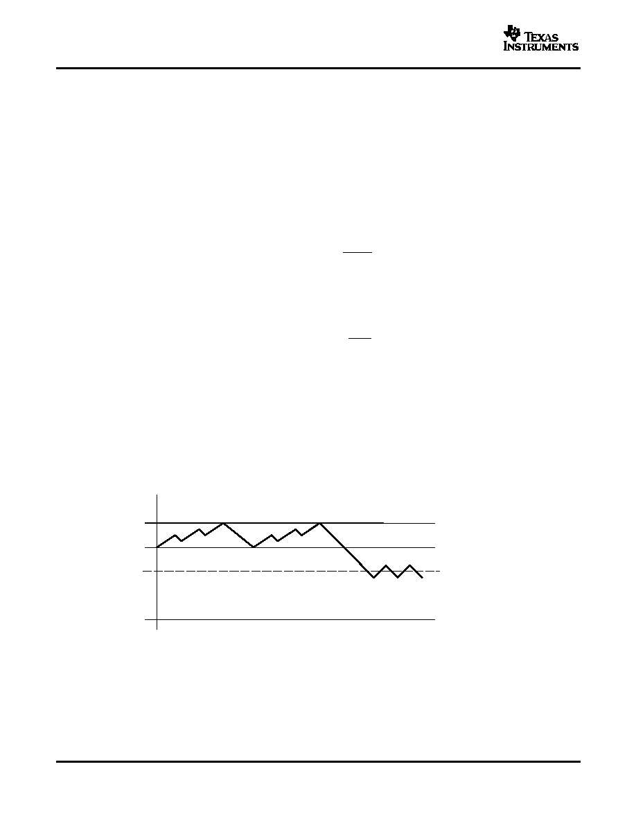
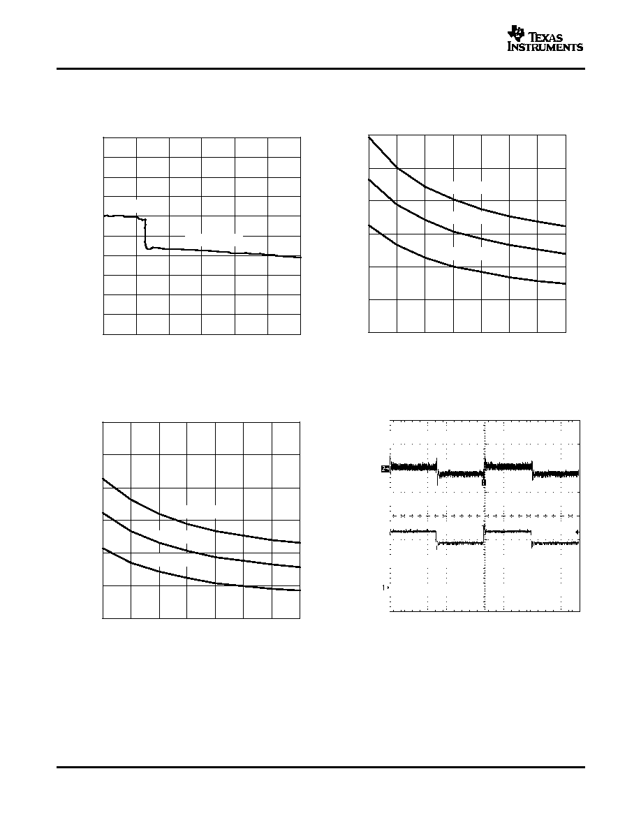
POWER SAVE MODE OPERATION
I
skip
v
66 mA
)
Vin
160
W
I
peak
+
66 mA
)
Vin
80
W
PFM Mode at Light Load
Comparator High
Comparator Low
Comparator Low 2
PWM Mode at Medium to Full Load
1.6%
0.8%
V
O
TPS62200, TPS62201
TPS62202, TPS62203, TPS62207
TPS62204, TPS62205, TPS62208
SLVS417D MARCH 2002 REVISED MAY 2004
DETAILED DESCRIPTION (continued)
The GM amplifier and input voltage determines the rise time of the Sawtooth generator; therefore any change in
input voltage or output voltage directly controls the duty cycle of the converter. This gives a very good line and
load transient regulation.
As the load current decreases, the converter enters the power save mode operation. During power save mode,
the converter operates with reduced switching frequency in PFM mode and with a minimum quiescent current to
maintain high efficiency.
Two conditions allow the converter to enter the power save mode operation. One is when the converter detects
the discontinuous conduction mode. The other is when the peak switch current in the P-channel switch goes
below the skip current limit. The typical skip current limit can be calculated as
During the power save mode the output voltage is monitored with the comparator by the thresholds comp low
and comp high. As the output voltage falls below the comp low threshold set to typically 0.8% above Vout
nominal, the P-channel switch turns on. The P-channel switch is turned off as the peak switch current is reached.
The typical peak switch current can be calculated:
The N-channel rectifier is turned on and the inductor current ramps down. As the inductor current approaches
zero the N-channel rectifier is turned off and the P-channel switch is turned on again, starting the next pulse. The
converter continues these pulses until the comp high threshold (set to typically 1.6% above Vout nominal) is
reached. The converter enters a sleep mode, reducing the quiescent current to a minimum. The converter wakes
up again as the output voltage falls below the comp low threshold again. This control method reduces the
quiescent current typically to 15 µA and reduces the switching frequency to a minimum, thereby achieving the
high converter efficiency. Setting the skip current thresholds to typically 0.8% and 1.6% above the nominal output
voltage at light load current results in a dynamic output voltage achieving lower absolute voltage drops during
heavy load transient changes. This allows the converter to operate with a small output capacitor of just 10 µF
and still have a low absolute voltage drop during heavy load transient changes. Refer to Figure 2 for detailed
operation of the power save mode.
Figure 2. Power Save Mode Thresholds and Dynamic Voltage Positioning
The converter enters the fixed frequency PWM mode again as soon as the output voltage falls below the comp
low 2 threshold.
4

www.ti.com
DYNAMIC VOLTAGE POSITIONING
SOFT START
LOW DROPOUT OPERATION 100% DUTY CYCLE
Vin
min
+
Vout
max
)
Iout
max
r
ds
(ON)
max
)
R
L
Iout
max
= maximum output current plus inductor ripple current
r
ds
(ON)
max
= maximum P-channel switch r
ds
(ON)
R
L
= DC resistance of the inductor
Vout
max
= nominal output voltage plus maximum output voltage tolerance
ENABLE
UNDERVOLTAGE LOCKOUT
TPS62200, TPS62201
TPS62202, TPS62203, TPS62207
TPS62204, TPS62205, TPS62208
SLVS417D MARCH 2002 REVISED MAY 2004
DETAILED DESCRIPTION (continued)
As described in the power save mode operation sections and as detailed in Figure 2, the output voltage is
typically 0.8% above the nominal output voltage at light load currents, as the device is in power save mode. This
gives additional headroom for the voltage drop during a load transient from light load to full load. During a load
transient from full load to light load, the voltage overshoot is also minimized due to active regulation turning on
the N-channel rectifier switch.
The TPS6220x has an internal soft start circuit that limits the inrush current during start-up. This prevents
possible voltage drops of the input voltage in case a battery or a high impedance power source is connected to
the input of the TPS6220x.
The soft start is implemented as a digital circuit increasing the switch current in steps of typically 60 mA,120 mA,
240 mA and then the typical switch current limit of 480 mA. Therefore the start-up time mainly depends on the
output capacitor and load current. Typical start-up time with 10 µF output capacitor and 200 mA load current is
800 µs.
The TPS6220x offers a low input to output voltage difference, while still maintaining operation with the 100% duty
cycle mode. In this mode, the P-channel switch is constantly turned on. This is particularly useful in battery
powered applications to achieve longest operation time by taking full advantage of the whole battery voltage
range. The minimum input voltage to maintain regulation, depending on the load current and output voltage, can
be calculated as
Pulling the enable low forces the part into shutdown, with a shutdown quiescent current of typically 0.1 µA. In this
mode, the P-channel switch and N-channel rectifier are turned off, the internal resistor feedback divider is
disconnected, and the whole device is in shutdown mode. If an output voltage, which could be an external
voltage source or super cap, is present during shutdown, the reverse leakage current is specified under electrical
characteristics. For proper operation the enable pin must be terminated and must not be left floating.
Pulling the enable high starts up the TPS6220x with the soft start as previously described.
The undervoltage lockout circuit prevents the device from misoperation at low input voltages. It prevents the
converter from turning on the switch or rectifier MOSFET under undefined conditions.
5
www.ti.com
ABSOLUTE MAXIMUM RATINGS
DISSIPATION RATING TABLE
RECOMMENDED OPERATING CONDITIONS
ELECTRICAL CHARACTERISTICS
TPS62200, TPS62201
TPS62202, TPS62203, TPS62207
TPS62204, TPS62205, TPS62208
SLVS417D MARCH 2002 REVISED MAY 2004
over operating free-air temperature (unless otherwise noted)
(1)
UNIT
Supply voltages, V
I
(2)
-0.3 V to 7.0 V
Voltages on pins SW, EN, FB
(2)
-0.3 V to V
CC
+0.3 V
Continuous power dissipation, P
D
See Dissipation Rating Table
Operating junction temperature range, T
J
-40
°
C to 150
°
C
Storage temperature, T
stg
-65
°
C to 150
°
C
Lead temperature (soldering, 10 sec)
260
°
C
(1)
Stresses beyond those listed under "absolute maximum ratings" may cause permanent damage to the device. These are stress ratings
only, and functional operation of the device at these or any other conditions beyond those indicated under "recommended operating
conditions" is not implied. Exposure to absolute-maximum-rated conditions for extended periods may affect device reliability.
(2)
All voltage values are with respect to network ground terminal.
T
A
25
°
C
T
A
= 70
°
C
T
A
= 85
°
C
PACKAGE
R
JA
POWER RATING
POWER RATING
POWER RATING
DBV
250
°
/W
400 mW
220 mW
160 mW
MIN
NOM
MAX
UNIT
Supply voltage, V
I
2.5
6.0
V
Output voltage range for adjustable output voltage version, V
O
0.7
V
I
V
Output current, I
O
300
mA
Inductor, L
(1)
4.7
10
µH
Input capacitor, C
I
(1)
4.7
µF
Output capacitor, C
O
(1)
10
µF
Operating ambient temperature, T
A
40
85
°
C
Operating junction temperature, T
J
40
125
°
C
(1)
See the application section for further information.
V
I
= 3.6 V, V
O
= 1.8 V, I
O
= 200 mA, EN = VIN, T
A
= -40
°
C to 85
°
C, typical values are at T
A
= 25
°
C (unless otherwise noted)
PARAMETER
TEST CONDITIONS
MIN
TYP
MAX
UNIT
SUPPLY CURRENT
V
I
Input voltage range
2.5
6.0
V
I
Q
Operating quiescent current
I
O
= 0 mA, Device is not switching
15
30
µA
Shutdown supply current
EN = GND
0.1
1
µA
Undervoltage lockout threshold
1.5
2.0
V
ENABLE
V
(EN)
EN high level input voltage
1.3
V
EN low level input voltage
0.4
V
I
(EN)
EN input bias current
EN = GND or VIN
0.01
0.1
µA
POWER SWITCH
V
IN
= V
GS
= 3.6 V
530
690
P-channel MOSFET on-resistance
m
V
IN
= V
GS
= 2.5 V
670
850
r
ds
(ON)
V
IN
= V
GS
= 3.6 V
430
540
N-channel MOSFET on-resistance
m
V
IN
= V
GS
= 2.5 V
530
660
6
www.ti.com
TPS62200, TPS62201
TPS62202, TPS62203, TPS62207
TPS62204, TPS62205, TPS62208
SLVS417D MARCH 2002 REVISED MAY 2004
ELECTRICAL CHARACTERISTICS (continued)
V
I
= 3.6 V, V
O
= 1.8 V, I
O
= 200 mA, EN = VIN, T
A
= -40
°
C to 85
°
C, typical values are at T
A
= 25
°
C (unless otherwise noted)
PARAMETER
TEST CONDITIONS
MIN
TYP
MAX
UNIT
SUPPLY CURRENT
I
lkg_(P)
P-channel leakage current
V
DS
= 6.0 V
0.1
1
µA
I
lkg_(N)
N-channel leakage current
V
DS
= 6.0 V
0.1
1
µA
I
(LIM)
P-channel current limit
2.5 V < Vin < 6.0 V
380
480
670
mA
OSCILLATOR
f
S
Switching frequency
650
1000
1500
kHz
OUTPUT
Adjustable output voltage
V
O
TPS62200
0.7
V
IN
V
range
V
ref
Reference voltage
0.5
V
TPS62200
V
I
= 3.6 V to 6.0 V, I
O
= 0 mA
0%
3%
Feedback voltage
(1)
Adjustable
V
I
= 3.6 V to 6.0 V, 0 mA
I
O
300 mA
-3%
3%
TPS62207
V
I
= 2.5 V to 6.0 V, I
O
= 0 mA
0%
3%
1.2 V
V
I
= 2.5 V to 6.0 V, 0 mA
I
O
300 mA
0%
3%
TPS62201
V
I
= 2.5 V to 6.0 V, I
O
= 0 mA
0%
3%
1.5 V
V
I
= 2.5 V to 6.0 V, 0 mA
I
O
300 mA
-3%
3%
TPS62204
V
I
= 2.5 V to 6.0 V, I
O
= 0 mA
0%
3%
1.6 V
V
I
= 2.5 V to 6.0 V, 0 mA
I
O
300 mA
-3%
3%
TPS62202
V
I
= 2.5 V to 6.0 V, I
O
= 0 mA
0%
3%
V
O
Fixed output voltage
(1)
1.8 V
V
I
= 2.5 V to 6.0 V, 0 mA
I
O
300 mA
-3%
3%
TPS62208
V
I
= 2.5 V to 6.0 V, I
O
= 0 mA
0%
3%
1.875 V
V
I
= 2.5 V to 6.0 V, 0 mA
I
O
300 mA
-3%
3%
TPS62205
V
I
= 2.7 V to 6.0 V, I
O
= 0 mA
0%
3%
2.5 V
V
I
= 2.7 V to 6.0 V, 0 mA
I
O
300 mA
-3%
3%
TPS62203
V
I
= 3.6 V to 6.0 V, I
O
= 0 mA
0%
3%
3.3 V
V
I
= 3.6 V to 6.0 V, 0 mA
I
O
300 mA
-3%
3%
Line regulation
V
I
= 2.5 V to 6.0 V, I
O
= 10 mA
0.26
%/V
Load regulation
I
O
= 100 mA to 300 mA
0.0014
%/mA
I
lkg
Leakage current into SW pin
Vin > Vout, 0 V
Vsw
Vin
0.1
1
µA
I
lkg
(Rev)
Reverse leakage current into pin SW
Vin = open, EN=GND, V
SW
= 6.0 V
0.1
1
µA
(1)
For output voltages
1.2 V a 22 µF output capacitor value is required to achieve a maximum output voltage accuracy of 3% while
operating in power save mode (PFM mode)
7
www.ti.com
TYPICAL CHARACTERISTICS
Table of Graphs
40
45
50
55
60
65
70
75
80
85
90
95
100
0.010
0.100
1
10
100
1000
V
O
= 3.3 V
V
I
= 3.7 V
V
I
= 5 V
Efficency - %
I
L
- Load Current - mA
40
45
50
55
60
65
70
75
80
85
90
95
100
0.010
0.100
1
10
100
1000
Efficiency - %
I
L
-Load Current - mA
V
O
= 1.8 V
V
I
= 2.7 V
V
I
= 3.7 V
V
I
= 5 V
TPS62200, TPS62201
TPS62202, TPS62203, TPS62207
TPS62204, TPS62205, TPS62208
SLVS417D MARCH 2002 REVISED MAY 2004
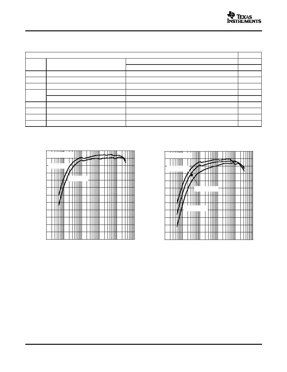
FIGURES
vs Load current
3,4,5
Efficiency
vs Input voltage
6
I
Q
No load quiescent current
vs Input voltage
7
f
s
Switching frequency
vs Temperature
8
V
o
Output voltage
vs Output current
9
r
ds
(on) - P-channel switch,
vs Input voltage
10
r
ds
(on)
r
ds
(on) - N-Channel rectifier switch
vs Input voltage
11
Line transient response
12
Load transient response
13
Power save mode operation
14
Start-up
15
EFFICIENCY
EFFICIENCY
vs
vs
LOAD CURRENT
LOAD CURRENT
Figure 3.
Figure 4.
8
www.ti.com
40
45
50
55
60
65
70
75
80
85
90
95
100
0.010
0.100
1
10
100
1000
V
O
= 1.5 V
V
I
= 2.7 V
V
I
= 5 V
Efficency - %
I
L
- Load Current - mA
V
I
= 3.7V
70
75
80
85
90
95
100
2.50
3
3.50
4
4.50
5
5.50
6
V
O
= 1.8 V
I
L
= 150 mA
I
L
= 1 mA
I
L
= 300 mA
Efficiency - %
V
I
- Input Voltage - V
0
5
10
15
20
25
2.50
3
3.50
4
4.50
5
5.50
6
T
A
= 85
°
C
T
A
= 25
°
C
T
A
= -40
°
C
N0 Load Quiescent Current -
V
I
- Input Voltage - V
A
µ
1025
1030
1035
1040
1045
1050
1055
1060
1065
1070
1075
1080
-40 -30 -20 -10
0 10 20 30 40 50 60 70 80
f - Frequency - kHz
T
A
- Temperature -
°
C
V
I
= 3.6 V
V
I
= 6 V
V
I
= 2.5 V
TPS62200, TPS62201
TPS62202, TPS62203, TPS62207
TPS62204, TPS62205, TPS62208
SLVS417D MARCH 2002 REVISED MAY 2004
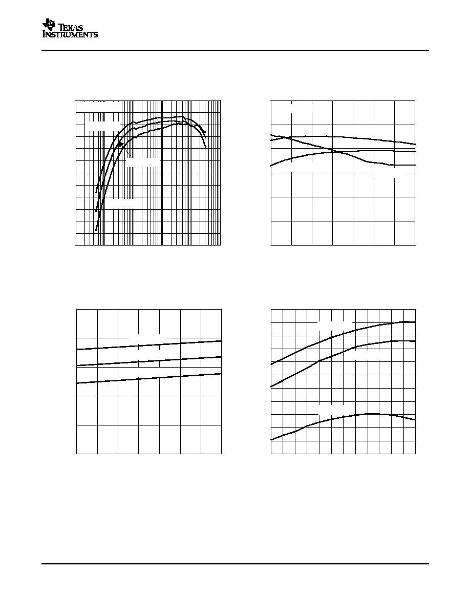
TYPICAL CHARACTERISTICS (continued)
EFFICIENCY
EFFICIENCY
vs
vs
LOAD CURRENT
INPUT VOLTAGE
Figure 5.
Figure 6.
NO LOAD QUIESCENT CURRENT
FREQUENCY
vs
vs
INPUT VOLTAGE
TEMPERATURE
Figure 7.
Figure 8.
9
www.ti.com
0.2
0.3
0.4
0.5
0.6
0.7
0.8
2.5
3
3.5
4
4.5
5
5.5
6
T
A
= 85
°
C
T
A
= 25
°
C
T
A
= -40
°
C
V
I
- Input Voltage - V
r ds(on)
- P-Channel Switch -
1.70
1.72
1.74
1.76
1.78
1.80
1.82
1.84
1.86
1.88
1.90
0
50
100
150
200
250
300
- Outrput V
oltage - V
V
O
I
O
- Output Current - mA
PFM Mode
PWM Mode
V
O
20 mV/div
V
I
3.6 V to 4.6 V
200
µ
s/div
0.2
0.3
0.4
0.5
0.6
0.7
0.8
2.5
3
3.5
4
4.5
5
5.5
6
T
A
= 85
°
C
T
A
= 25
°
C
T
A
= -40
°
C
V
I
- Input Voltage - V
rDS
(on)
N-Channel Switch --
TPS62200, TPS62201
TPS62202, TPS62203, TPS62207
TPS62204, TPS62205, TPS62208
SLVS417D MARCH 2002 REVISED MAY 2004
TYPICAL CHARACTERISTICS (continued)
OUTPUT VOLTAGE
r
ds
(on) P-CHANNEL SWITCH
vs
vs
OUTPUT CURRENT
INPUT VOLTAGE
Figure 9.
Figure 10.
r
ds
(on) P-CHANNEL SWITCH
vs
INPUT VOLTAGE
LINE TRANSIENT RESPONSE
Figure 11.
Figure 12.
10
www.ti.com
V
O
50 mV/div
I
O
3 mA to 270 mA
100
µ
s/div
V
SW
5 V/div
I
L
100 mA/div
V
O
20 mV/div
2
µ
s/div
V
O
= 1.8 V/200 mA
Enable
2 V/div
I
L
50 mA/div
V
O
1 V/div
100
µ
s/div
TPS62200, TPS62201
TPS62202, TPS62203, TPS62207
TPS62204, TPS62205, TPS62208
SLVS417D MARCH 2002 REVISED MAY 2004
TYPICAL CHARACTERISTICS (continued)
LOAD TRANSIENT RESPONSE
POWER SAVE MODE OPERATION
Figure 13.
Figure 14.
START-UP
Figure 15.
11
www.ti.com
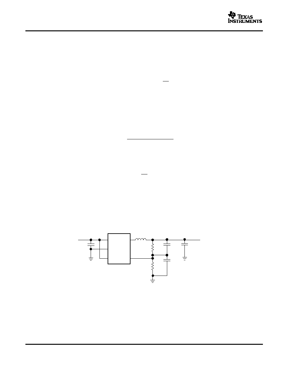
APPLICATION INFORMATION
ADJUSTABLE OUTPUT VOLTAGE VERSION
Vout
+
0.5 V
1
)
R1
R2
C1
+
1
2
p
10 kHz
R1
C2
+
R1
R2
C1
V
I
GND
EN
SW
FB
C3
4.7
µ
F
L1
10
µ
H
C4
10
µ
F
TPS62200
V
I
2.5 V - 6 V
V
O
1.8 V / 300 mA
R1
470k
R2
180k
C1
33 pF
C2
100 pF
INDUCTOR SELECTION
TPS62200, TPS62201
TPS62202, TPS62203, TPS62207
TPS62204, TPS62205, TPS62208
SLVS417D MARCH 2002 REVISED MAY 2004
When the adjustable output voltage version TPS62200 is used, the output voltage is set by the external resistor
divider. See Figure 16.
The output voltage is calculated as
·
R1 + R2
1 M
and internal reference voltage V(ref)typ = 0.5 V
R1 + R2 should not be greater than 1 M
for reasons of stability. To keep the operating quiescent current to a
minimum, the feedback resistor divider should have high impedance with R1+R2
1 M
. Because of the high
impedance and the low reference voltage of V
ref
= 0.5 V, the noise on the feedback pin (FB) needs to be
minimized. Using a capacitive divider C1 and C2 across the feedback resistors minimizes the noise at the
feedback without degrading the line or load transient performance.
C1 and C2 should be selected as
·
R1 = upper resistor of voltage divider
·
C1 = upper capacitor of voltage divider
For C1 a value should be chosen that comes closest to the calculated result.
·
R2 = lower resistor of voltage divider
·
C2 = lower capacitor of voltage divider
For C2 the selected capacitor value should always be selected larger than the calculated result. For example, in
Figure 16 for C2, 100 pF are selected for a calculated result of C2 = 86.17 pF.
If quiescent current is not a key design parameter, C1 and C2 can be omitted, and a low-impedance feedback
divider must be used with R1+R2 <100 k
. This design reduces the noise available on the feedback pin (FB) as
well, but increases the overall quiescent current during operation.
Figure 16. Typical Application Circuit for the Adjustable Output Voltage
The TPS6220x device is optimized to operate with a typical inductor value of 10 µH.
For high efficiencies, the inductor should have a low dc resistance to minimize conduction losses. Although the
inductor core material has less effect on efficiency than its dc resistance, an appropriate inductor core material
must be used.
12
www.ti.com
D
I
L
+
Vout
1 Vout
Vin
L
f
I
Lmax
+
I
outmax
)
D
I
L
2
f = switching frequency (1 MHz typical, 650 kHz minimal)
L = inductor valfue
I
L
= peak-to-peak inductor ripple current
I
Lmax
= maximum inducator current
INPUT CAPACITOR SELECTION
OUTPUT CAPACITOR SELECTION
TPS62200, TPS62201
TPS62202, TPS62203, TPS62207
TPS62204, TPS62205, TPS62208
SLVS417D MARCH 2002 REVISED MAY 2004
APPLICATION INFORMATION (continued)
The inductor value determines the inductor ripple current. The larger the inductor value, the smaller the inductor
ripple current, and the lower the conduction losses of the converter. On the other hand, larger inductor values
cause a slower load transient response. Usually the inductor ripple current, as calculated below, is around 20%
of the average output current.
In order to avoid saturation of the inductor, the inductor should be rated at least for the maximum output current
of the converter plus the inductor ripple current that is calculated as
The highest inductor current occurs at maximum Vin.
A more conservative approach is to select the inductor current rating just for the maximum switch current of
670 mA. Refer to Table 1 for inductor recommendations.
Table 1. Recommended Inductors
INDUCTOR VALUE
COMPONENT SUPPLIER
COMMENTS
10 µH
Sumida CDRH5D28-100
High efficiency
10 µH
Sumida CDRH5D18-100
10 µH
Sumida CDRH4D28-100
10 µH
Coilcraft DO1608-103
6.8 µH
Sumida CDRH3D16-6R8
Smallest solution
10 µH
Sumida CDRH4D18-100
10 µH
Sumida CR32-100
10 µH
Sumida CR43-100
10 µH
Murata LQH4C100K04
Because the buck converter has a pulsating input current, a low ESR input capacitor is required. This results in
the best input voltage filtering and minimizing the interference with other circuits caused by high input voltage
spikes. Also the input capacitor must be sufficiently large to stabilize the input voltage during heavy load
transients. For good input voltage filtering, usually a 4.7 µF input capacitor is sufficient. It can be increased
without any limit for better input-voltage filtering. If ceramic output capacitors are used, the capacitor RMS ripple
current rating always meets the application requirements.
Ceramic capacitors show a good performance because of the low ESR value, and they are less sensitive against
voltage transients and spikes compared to tantalum capacitors.
Place the input capacitor as close as possible to the input pin of the device for best performance (refer to Table 2
for recommended components).
The advanced fast response voltage mode control scheme of the TPS6220x allows the use of tiny ceramic
capacitors with a value of 10 µF without having large output voltage under and overshoots during heavy load
transients.
Ceramic capacitors with low ESR values have the lowest output voltage ripple and are therefore recommended.
If required, tantalum capacitors may be used as well (refer to Table 2 for recommended components).
13
www.ti.com
D
Vout
+
Vout
1 Vout
Vin
L
f
1
8
Cout
f
)
ESR
LAYOUT CONSIDERATIONS
V
I
GND
EN
SW
FB
C1
4.7
µ
F
L1
10
µ
H
C2
10
µ
F
TPS62200
V
I
2.5 V - 6 V
V
O
1.8 V / 300 mA
R1
R2
Cff
TPS62200, TPS62201
TPS62202, TPS62203, TPS62207
TPS62204, TPS62205, TPS62208
SLVS417D MARCH 2002 REVISED MAY 2004
At nominal load current the device operates in PWM mode and the overall output voltage ripple is the sum of the
voltage spike caused by the output capacitor ESR plus the voltage ripple caused by charging and discharging the
output capacitor:
where the highest output voltage ripple occurs at the highest input voltage Vin.
At light load currents, the device operates in power save mode, and the output voltage ripple is independent of
the output capacitor value. The output voltage ripple is set by the internal comparator thresholds. The typical
output voltage ripple is 1% of the output voltage Vo.
Table 2. Recommended Capacitors
CAPACITOR VALUE
CASE SIZE
COMPONENT SUPPLIER
COMMENTS
4.7 µF
0805
Taiyo Yuden JMK212BY475MG
Ceramic
10 µF
0805
Taiyo Yuden JMK212BJ106MG
Ceramic
TDK C12012X5ROJ106K
Ceramic
10 µF
1206
Taiyo Yuden JMK316BJ106KL
Ceramic
TDK C3216X5ROJ106M
22 µF
1210
Taiyo Yuden JMK325BJ226MM
Ceramic
For all switching power supplies, the layout is an important step in the design, especially at high peak currents
and switching frequencies. If the layout is not carefully done, the regulator shows stability problems as well as
EMI problems.
Therefore use wide and short traces for the main current paths, as indicated in bold in Figure 17. The input
capacitor, as well as the inductor and output capacitor, should be placed as close as possible to the IC pins
The feedback resistor network must be routed away from the inductor and switch node to minimize noise and
magnetic interference. To further minimize noise from coupling into the feedback network and feedback pin, the
ground plane or ground traces must be used for shielding. This becomes very important especially at high
switching frequencies of 1 MHz.
Figure 17. Layout Diagram
14
www.ti.com
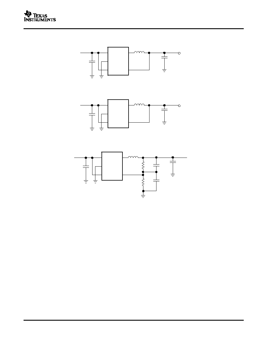
TYPICAL APPLICATIONS
V
I
GND
EN
SW
FB
C1
4.7
µ
F
L1
10
µ
H
C2
10
µ
F
TPS62202
V
I
2.5 V to 6 V
V
O
1.8 V/300 mA
1
2
3
5
4
V
I
GND
EN
SW
FB
C1
4.7
µ
F
L1
4.7
µ
H
C2
22
µ
F
TPS62202
V
I
2.5 V to 6 V
V
O
1.8 V/300 mA
1
2
3
5
4
V
I
GND
EN
SW
FB
C3
4.7
µ
F
L1
10
µ
H
C4
10
µ
F
TPS62200
V
I
2.5 V to 6 V
V
O
1.5 V/300 mA
R1
360 k
R2
180 k
C1
47 pF
C2
100 pF
1
2
3
5
4
TPS62200, TPS62201
TPS62202, TPS62203, TPS62207
TPS62204, TPS62205, TPS62208
SLVS417D MARCH 2002 REVISED MAY 2004
Figure 18. Li-Ion to 1.8 V Fixed Output Voltage Version
Figure 19. 1.8 V Fixed Output Voltage version Using 4.7µH Inductor
Figure 20. Adjustable Output Voltage Version Set to 1.5 V
15

IMPORTANT NOTICE
Texas Instruments Incorporated and its subsidiaries (TI) reserve the right to make corrections, modifications,
enhancements, improvements, and other changes to its products and services at any time and to discontinue
any product or service without notice. Customers should obtain the latest relevant information before placing
orders and should verify that such information is current and complete. All products are sold subject to TI's terms
and conditions of sale supplied at the time of order acknowledgment.
TI warrants performance of its hardware products to the specifications applicable at the time of sale in
accordance with TI's standard warranty. Testing and other quality control techniques are used to the extent TI
deems necessary to support this warranty. Except where mandated by government requirements, testing of all
parameters of each product is not necessarily performed.
TI assumes no liability for applications assistance or customer product design. Customers are responsible for
their products and applications using TI components. To minimize the risks associated with customer products
and applications, customers should provide adequate design and operating safeguards.
TI does not warrant or represent that any license, either express or implied, is granted under any TI patent right,
copyright, mask work right, or other TI intellectual property right relating to any combination, machine, or process
in which TI products or services are used. Information published by TI regarding third-party products or services
does not constitute a license from TI to use such products or services or a warranty or endorsement thereof.
Use of such information may require a license from a third party under the patents or other intellectual property
of the third party, or a license from TI under the patents or other intellectual property of TI.
Reproduction of information in TI data books or data sheets is permissible only if reproduction is without
alteration and is accompanied by all associated warranties, conditions, limitations, and notices. Reproduction
of this information with alteration is an unfair and deceptive business practice. TI is not responsible or liable for
such altered documentation.
Resale of TI products or services with statements different from or beyond the parameters stated by TI for that
product or service voids all express and any implied warranties for the associated TI product or service and
is an unfair and deceptive business practice. TI is not responsible or liable for any such statements.
Following are URLs where you can obtain information on other Texas Instruments products and application
solutions:
Products
Applications
Amplifiers
amplifier.ti.com
Audio
www.ti.com/audio
Data Converters
dataconverter.ti.com
Automotive
www.ti.com/automotive
DSP
dsp.ti.com
Broadband
www.ti.com/broadband
Interface
interface.ti.com
Digital Control
www.ti.com/digitalcontrol
Logic
logic.ti.com
Military
www.ti.com/military
Power Mgmt
power.ti.com
Optical Networking
www.ti.com/opticalnetwork
Microcontrollers
microcontroller.ti.com
Security
www.ti.com/security
Telephony
www.ti.com/telephony
Video & Imaging
www.ti.com/video
Wireless
www.ti.com/wireless
Mailing Address:
Texas Instruments
Post Office Box 655303 Dallas, Texas 75265
Copyright
2004, Texas Instruments Incorporated
Document Outline