Actual Size
(2,15 mm x 2,3 mm)
www.ti.com
FEATURES
DESCRIPTION
APPLICATIONS
3
2
4
5
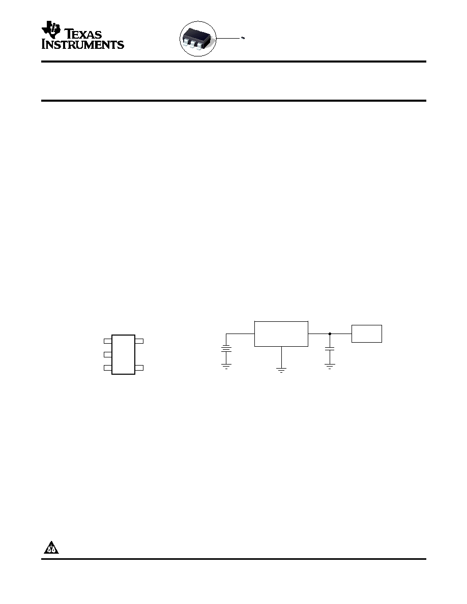
DCK PACKAGE
(TOP VIEW)
1
FB/NC
GND
NC
OUT
IN
TPS715xx
OUT
IN
MSP430
Li
-
TPS71501
TPS71525, TPS71530
TPS71533, TPS71550
SLVS338H MAY 2001 REVISED JUNE 2004
50 mA, 24 V, 3.2µA Supply Current
Low-Dropout Linear Regulator in SC70 Package
·
24-V Maximum Input Voltage
The TPS715xx low-dropout (LDO) voltage regulators
offer the benefits of high input voltage, low-dropout
·
Low 3.2-µA Quiescent Current at 50 mA
voltage, low-power operation, and miniaturized pack-
·
Stable With Any Capacitor (> 0.47 µF)
aging. The devices, which operate over an input
·
50-mA Low-Dropout Regulator
range of 2.5 V to 24 V, are stable with any capacitor
·
Available in 2.5 V, 3.0 V, 3.3 V, 5.0 V, and
(> 0.47 µF). The low dropout voltage and low
quiescent current allow operations at extremely low
Adjustable (12 V to 15 V)
power levels. Therefore, the devices are ideal for
·
Minimum/Maximum Specified Current Limit
powering battery management ICs. Specifically, since
·
5-Pin SC70/SOT-323 (DCK) Package
the devices are enabled as soon as the applied
voltage reaches the minimum input voltage, the
·
-40
°
C to 125
°
C Specified Junction
output is quickly available to power continuously
Temperature Range
operating battery charging ICs.
The usual PNP pass transistor has been replaced by
·
Ultra Low Power Microcontrollers
a PMOS pass element. Because the PMOS pass
element behaves as a low-value resistor, the low
·
Cellular/Cordless Handsets
dropout voltage, typically 415 mV at 50 mA of load
·
Portable/Battery-Powered Equipment
current, is directly proportional to the load current.
The low quiescent current (3.2 µA typically) is stable
over the entire range of output load current (0 mA to
50 mA).
Please be aware that an important notice concerning availability, standard warranty, and use in critical applications of Texas
Instruments semiconductor products and disclaimers thereto appears at the end of this data sheet.
PRODUCTION DATA information is current as of publication date.
Copyright © 20012004, Texas Instruments Incorporated
Products conform to specifications per the terms of the Texas
Instruments standard warranty. Production processing does not
necessarily include testing of all parameters.
www.ti.com
ABSOLUTE MAXIMUM RATINGS
DISSIPATION RATING TABLE
TPS71501
TPS71525, TPS71530
TPS71533, TPS71550
SLVS338H MAY 2001 REVISED JUNE 2004
AVAILABLE OPTIONS
(1)
T
J
VOLTAGE
PACKAGE
PART NUMBER
SYMBOL
2.5 V
SC70/SOT-323 (DCK)
TPS71525DCKR
AQL
3.0 V
SC70/SOT-323 (DCK)
TPS71530DCKR
AQM
-40
°
C to 125
°
C
3.3 V
SC70/SOT-323 (DCK)
TPS71533DCKR
AQI
5.0 V
SC70/SOT-323 (DCK)
TPS71550DCKR
T48
(Adjustable) 1.2 V-15 V
SC70/SOT-323 (DCK)
TPS71501DCKR
ARB
(1)
Contact the factory for other voltage options between 1.25 V and 5.85 V.
over operating temperature range (unless otherwise noted)
(1) (2)
UNIT
V
IN
range
-0.3 V to 24 V
Peak output current
Internally limited
ESD rating, HBM
2 kV
ESD rating, CDM
500 V
Continuous total power dissipation
See Dissipation Rating Table
Junction temperature range, T
J
-40
°
C to 150
°
C
Storage temperature range, T
stg
-65
°
C to 150
°
C
(1)
Stresses beyond those listed under absolute maximum ratings may cause permanent damage to the device. These are stress ratings
only, and functional operation of the device at these or any other conditions beyond those indicated under recommended operating
conditions is not implied. Exposure to absolute-maximum-rated conditions for extended periods may affect device reliability.
(2)
All voltage values are with respect to network ground terminal.
DERATING FACTOR
T
A
25
°
C
T
A
= 70
°
C
T
A
= 85
°
C
BOARD
PACKAGE
R
JC
°
C/W
R
JA
°
C/W
ABOVE T
A
= 25
°
C
POWER RATING
POWER RATING
POWER RATING
Low-K
(1)
DCK
165
395
2.52 mW/
°
C
250 mW
140 mW
100 mW
High-K
(2)
DCK
165
315
3.18 mW/
°
C
320 mW
175 mW
130 mW
(1)
The JEDEC Low-K (1s) board design used to derive this data was a 3 inch x 3 inch, two-layer board with 2 ounce copper traces on top
of the board.
(2)
The JEDEC High-K (2s2p) board design used to derive this data was a 3 inch x 3 inch, multilayer board with 1 ounce internal power and
ground planes and 2 ounce copper traces on top and bottom of the board.
2
www.ti.com
ELECTRICAL CHARACTERISTICS
TPS71501
TPS71525, TPS71530
TPS71533, TPS71550
SLVS338H MAY 2001 REVISED JUNE 2004
over operating junction temperature range (T
J
= -40
°
C to 125
°
C), V
IN
= V
OUT(NOM)
+ 1 V, I
OUT
= 1 mA, C
OUT
= 1 µF unless
otherwise noted. Typical values are at T
J
= 25
°
C.
PARAMETER
TEST CONDITIONS
MIN
TYP
MAX
UNIT
I
O
= 10 mA
2.5
24
Input voltage
(1)
V
IN
V
I
O
= 50 mA
3
24
V
OUT
voltage range (TPS71501)
1.2
15
V
V
IN
+ 1.0 V
V
IN
24 V
V
OUT
accuracy
(1)
Over V
IN
, I
OUT
, and T
-4.0
+4.0
%
100 µA
I
OUT
50 mA
0
I
OUT
50 mA, T
J
= -40
°
C to +85
°
C
3.2
4.2
Ground pin current
I
GND
0 mA
I
OUT
50 mA
3.2
4.8
µA
0 mA
I
OUT
50 mA, V
IN
= 24 V
5.8
Load regulation
V
OUT
/
I
OUT
I
OUT
= 100 µA to 50 mA
22
mV
Output voltage
V
OUT
/
V
IN
V
OUT
+ 1 V < V
IN
24 V
20
60
mV
line regulation
(1)
BW = 200 Hz to 100 kHz, C
OUT
= 10 µF,
Output noise voltage
V
n
575
µVrms
I
OUT
= 50 mA
Output current limit
I
CL
V
O
= 0 V
125
750
mA
Power-supply ripple rejection
PSRR
f = 100 kHz, C
OUT
= 10 µF
60
dB
Dropout voltage
V
DO
I
OUT
= 50 mA
415
750
mV
V
IN
= V
OUT(NOM)
- 1 V
(1)
Minimum V
IN
= V
OUT
+ V
DO
or the value shown for Input voltage in this table, whichever is greater.
3
www.ti.com
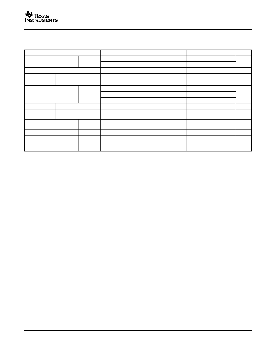
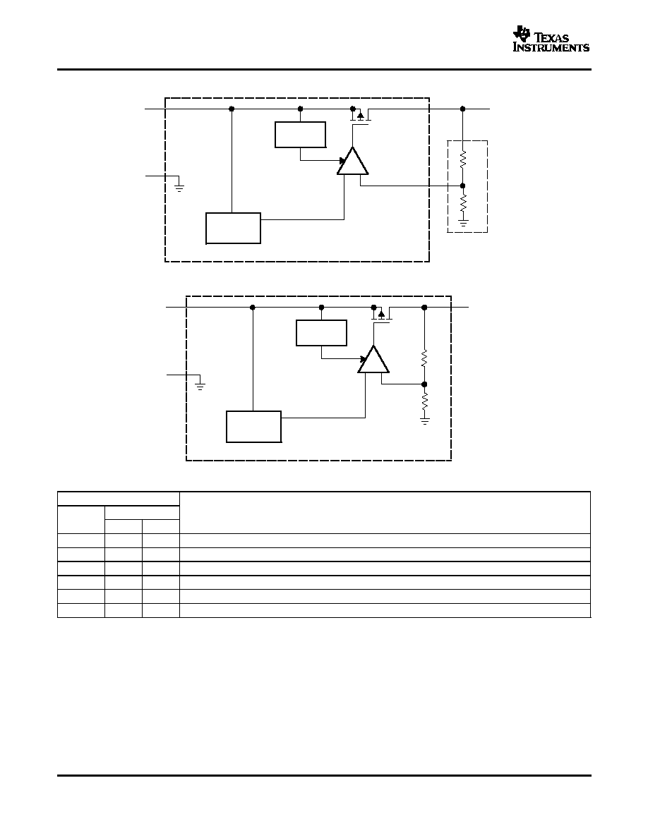
_
+
Current
Sense
R1
R2
V
(IN)
GND
V
(OUT)
ILIM
Bandgap
Reference
V
ref
= 1.205 V
FB
_
+
Current
Sense
R1
R2
V
(IN)
GND
V
(OUT)
ILIM
Bandgap
Reference
V
ref
= 1.205 V
R2 = 840 k
TPS71501
TPS71525, TPS71530
TPS71533, TPS71550
SLVS338H MAY 2001 REVISED JUNE 2004
FUNCTIONAL BLOCK DIAGRAM--ADJUSTABLE VERSION
FUNCTIONAL BLOCK DIAGRAM--FIXED VERSION
Table 1. Terminal Functions
TERMINAL
NO.
DESCRIPTION
NAME
FIXED
ADJ.
FB
1
Adjustable version. This terminal is used to set the output voltage.
NC
1
No connection
GND
2
2
Ground
NC
3
3
No connection
IN
4
4
Unregulated input supply.
OUT
5
5
Output of the regulator, any output capacitor
0.47 µF can be used for stability.
4