
TPS72101, TPS72115
TPS72116, TPS72118
SLVS352B ≠ DECEMBER 2001 ≠ REVISED MAY 2002
LOW INPUT VOLTAGE, CAP FREE 150-mA
LOW-DROPOUT LINEAR REGULATORS
(3,00 mm x 3,00 mm)
Actual Size
FEATURES
D
150-mA LDO
D
Available in 1.5-V, 1.6-V, 1.8-V Fixed-Output
and Adjustable Versions
D
Low Input Voltage Requirement
(Down to 1.8 V)
D
Small Output Capacitor, 0.1-
µ
F
D
Dropout Voltage Typically 200 mV at 150 mA
D
Less Than 1
µ
A Quiescent Current in
Shutdown Mode
D
Thermal Protection
D
Over Current Limitation
D
5-Pin SOT-23 (DBV) Package
APPLICATIONS
D
Portable Communication Devices
D
Battery Powered Equipment
D
PCMCIA Cards
D
Personal Digital Assistants
D
Modems
D
Bar Code Scanners
D
Backup Power Supplies
D
SMPS Post Regulation
D
Internet Audio
DESCRIPTION
The TPS721xx family of LDO regulators is available in
fixed voltage options that are commonly used to power
the latest DSP's and microcontrollers with an adjustable
option ranging from 1.22 V to 2.5 V. These regulators
can be used in a wide variety of applications ranging
from portable, battery-powered equipment to PC
peripherals. The family features operation over a wide
range of input voltages (1.8 V to 5.5 V) and low dropout
voltage (150 mV at full load). Therefore, compared to
many other regulators that require 2.5-V or higher input
voltages for operation, these regulators can be
operated directly from two AAA batteries. Also, the
typical quiescent current (ground pin current) is low,
starting at 85
µ
A during normal operation and 1
µ
A in
shutdown mode. These regulators can be operated
very efficiently and, in a battery-powered application,
help extend the longevity of the device.
Similar LDO regulators require 1-
µ
F or larger output
capacitors for stability. However, this regulator uses an
internal compensation scheme that stabilizes the
feedback loop over the full range of input voltages and
load currents with output capacitances as low as
0.1-
µ
F. Ceramic capacitors of this size are relatively
inexpensive and available in small footprints.
This family of regulators is particularly suited as a
portable power supply solution due to its minimal board
space requirement and 1.8-V minimum input voltage.
Being able to use two off-the-shelf, AAA, batteries
makes system design easier and also reduces
component cost. Moreover, the solution will be more
efficient than if a regulator with a higher input voltage is
used.
3
2
4
5
DBV PACKAGE
(TOP VIEW)
1
IN
GND
EN
OUT
NC/FB
TPS72115
0.1
µ
F
0.1
µ
F
1.8 V
1.5 V
GND
OUT
IN
EN
PRODUCTION DATA information is current as of publication date. Products
conform to specifications per the terms of Texas Instruments standard warranty.
Production processing does not necessarily include testing of all parameters.
Please be aware that an important notice concerning availability, standard warranty, and use in critical applications of Texas Instruments
semiconductor products and disclaimers thereto appears at the end of this data sheet.
www.ti.com
Copyright
2002, Texas Instruments Incorporated
TPS72101, TPS72115
TPS72116, TPS72118
SLVS352B ≠ DECEMBER 2001 ≠ REVISED MAY 2002
www.ti.com
2
These devices have limited built-in ESD protection. The leads should be shorted together or the device placed in conductive foam during
storage or handling to prevent electrostatic damage to the MOS gates.
ORDERING INFORMATION
TJ
VOLTAGE
PACKAGE
PART NUMBER
SYMBOL
Adjustable
TPS72101DBVT(1)
TPS72101DBVR(2)
PEKI
40
∞
C to 125
∞
C
1.5 V
SOT-23
TPS72115DBVT(1)
TPS72115DBVR(2)
PEII
≠40
∞
C to 125
∞
C
1.6 V
SOT 23
(DBV)
TPS72116DBVT(1)
TPS72116DBVR(2)
PHFI
1.8 V
TPS72118DBVT(1)
TPS72118DBVR(2)
PEJI
(1) The DBVT indicates tape and reel of 250 parts.
(2) The DBVR indicates tape and reel of 3000 parts.
ABSOLUTE MAXIMUM RATINGS
over operating free-air temperature range unless otherwise noted(1)
TPS72101, TPS72115
TPS72116, TPS72118
Input voltage range(2)
≠ 0.3 V to 7 V
Voltage range at EN
≠0.3 V to 7 V
Voltage on OUT, FB, NC
≠0.3 V to VI + 0.3 V
Peak output current
Internally limited
ESD rating, HBM
3 kV
Continuous total power dissipation
See Dissipation Rating Table
Operating virtual junction temperature range, TJ
≠ 40
∞
C to 150
∞
C
Storage temperature range, Tstg
≠ 65
∞
C to 150
∞
C
(1) Stresses beyond those listed under "absolute maximum ratings" may cause permanent damage to the device. These are stress ratings only, and
functional operation of the device at these or any other conditions beyond those indicated under "recommended operating conditions" is not
implied. Exposure to absolute-maximum-rated conditions for extended periods may affect device reliability.
(2) All voltage values are with respect to network ground terminal.
PACKAGE DISSIPATION RATING
BOARD
PACKAGE
R
JC
R
JA
DERATING FACTOR
ABOVE TA = 25
∞
C
TA
25
∞
C
POWER RATING
TA = 70
∞
C
POWER RATING
TA = 85
∞
C
POWER RATING
Low K(1)
DBV
65.8
∞
C/W
259
∞
C/W
3.9 mW/
∞
C
386 mW
212 mW
154 mW
High K(2)
DBV
65.8
∞
C/W
180
∞
C/W
5.6 mW/
∞
C
555 mW
305 mW
222 mW
(1) The JEDEC Low K (1s) board design used to derive this data was a 3 inch x 3 inch, two-layer board with 2 ounce copper traces on top of the board.
(2) The JEDEC High K (2s2p) board design used to derive this data was a 3 inch x 3 inch, multilayer board with 1 ounce internal power and ground
planes and 2 ounce copper traces on top and bottom of the board.
TPS72101, TPS72115
TPS72116, TPS72118
SLVS352B ≠ DECEMBER 2001 ≠ REVISED MAY 2002
www.ti.com
3
ELECTRICAL CHARACTERISTICS
over recommended operating free-air temperature range VI = VO(typ) + 1 V, IO= 1 mA, EN = VI, Co = 1
µ
F (unless otherwise noted)
PARAMETER
TEST CONDITIONS
MIN
TYP
MAX
UNIT
VI
Input voltage(1)
1.8
5.5
V
IO
Continuous output current
0
150
mA
TJ
Operating junction temperature
≠40
125
∞
C
TPS72101
0
µ
A< IO < 150 mA,(1)
1.8 V
VO
2.5 V
0.97 VO
1.03 VO
TPS72115
TJ = 25
∞
C
1.5
TPS72115
0
µ
A< IO < 150 mA,
2.5 V
VI
5.5 V
1.455
1.545
VO
Output voltage
TPS72116
TJ = 25
∞
C
1.6
V
VO
Out ut voltage
TPS72116
0
µ
A< IO < 150 mA,
2.6 V
VI
5.5 V
1.552
1.648
V
TPS72118
TJ = 25
∞
C
1.8
TPS72118
0
µ
A< IO < 150 mA,
2.8 V
VI
5.5 V
1.746
1.854
TJ = 25
∞
C
85
I
Quiescent current (GND current)
120
A
I(Q)
Quiescent current (GND current)
IO = 150 mA,
TJ = 25
∞
C
570
µ
A
IO = 150 mA
850
Standby current
EN < 0.5 V,
TJ = 25
∞
C
0.01
A
Standby current
EN < 0.5 V
1
µ
A
Vn
Output noise voltage
TPS72115
BW = 200 Hz to 100 kHz,
TJ = 25
∞
C,
Co = 1
µ
F
90
µ
V
Vref
Reference voltage
TJ = 25
∞
C
1.225
V
PSRR
Ripple rejection
f = 100 Hz, Co = 10
µ
F,
IO = 150 mA,
TJ = 25
∞
C,
See Note 1
48
dB
Current limit
See Note 2
175
525
mA
Output voltage line regulation
V
1 V
V
5 5 V
TJ = 25
∞
C
0.03
0.09
%/V
Out ut voltage line regulation
(
VO/VO)(3)
VO + 1 V < VI
5.5 V
0.1
%/V
Output voltage load
regulation
TPS72118
0 < IO < 150 mA,
TJ = 25
∞
C
0.5
mV
VIH
EN high level input
1.4
V
VIL
EN low level input
≠0.2
0.4
V
I
EN i
t
t
EN = 0 V
≠0.01
A
II
EN input current
EN = IN
≠0.01
µ
A
V
D
t
lt
(4)
TPS72118
IO = 150 mA,
TJ = 25
∞
C
150
V
VDO
Dropout voltage (4)
TPS72101
IO = 150 mA,
1.2 V
VO
5.2 V
240
mV
In
Feedback input current
TPS72101
1
µ
A
1
Thermal shutdown temperature
170
∞
C
Thermal shutdown hysteresis
20
∞
C
(1) Minimum IN operating voltage is 1.8 V or VO(max) + VDO (max load), whichever is greater.
(2) Test condition includes, output voltage VO=1 V and pulse duration = 10 mS.
(3) VImin = (VO + 1) or 1.8 V whichever is greater.
Line regulation (mV)
+
% V
V
O
5.5 V
*
V
Imin
100
1000
(4) Dropout voltage is defined as the differential voltage between VO and VI when VO drops 100 mV below the value measured with VI = VO + 1 V.

TPS72101, TPS72115
TPS72116, TPS72118
SLVS352B ≠ DECEMBER 2001 ≠ REVISED MAY 2002
www.ti.com
4
FUNCTIONAL BLOCK DIAGRAM--ADJUSTABLE VERSION
TPS72101
OUT
IN
FB
GND
EN
Vref
Current Limit
/ Thermal
Protection
FUNCTIONAL BLOCK DIAGRAM--FIXED VERSION
TPS72115/16/18
OUT
IN
GND
EN
Vref
Current Limit
/ Thermal
Protection
NC (see Note 1)
(1) This pin must be left floating and not connected to GND.
Terminal Functions
TERMINAL
I/O
DESCRIPTION
NAME
NO.
I/O
DESCRIPTION
GND
2
Ground
EN
3
I
Enable input
IN
1
I
Input supply voltage
NC/FB
4
I
NC = Not connected (see Note 6); FB = Feedback (adjustable option TPS72101)
OUT
5
O
Regulated output voltage
TPS72101, TPS72115
TPS72116, TPS72118
SLVS352B ≠ DECEMBER 2001 ≠ REVISED MAY 2002
www.ti.com
5
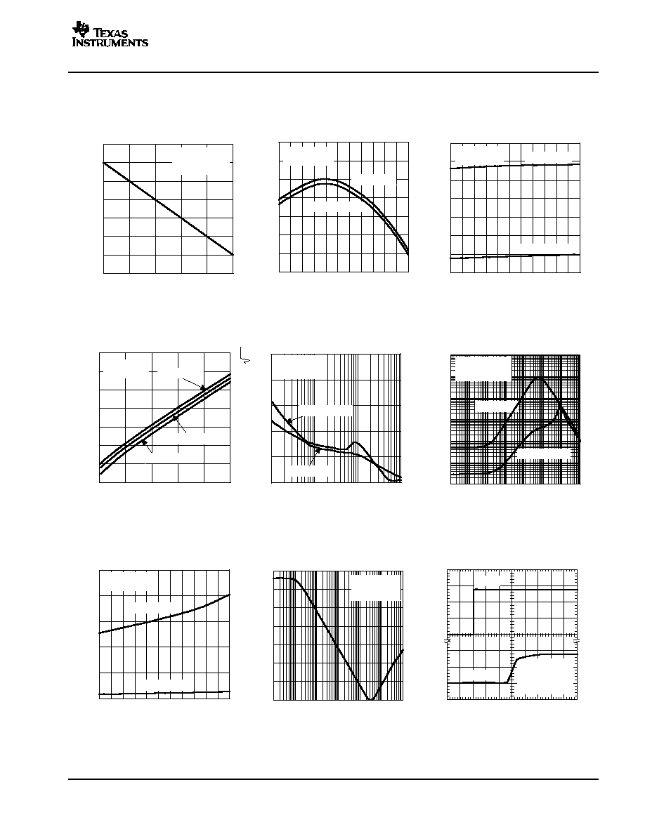
TYPICAL CHARACTERISTICS
Figure 1
1.7995
1.7996
1.7997
1.7998
1.7999
1.8000
1.8001
1.8002
0
30
60
90
120
150
IO ≠ Output Current ≠ mA
TPS72118
OUTPUT VOLTAGE
vs
OUTPUT CURRENT
≠
Output V
oltage
≠
V
V
O
VI = 2.8 V
Co = 1
µ
F
TJ = 25
∞
C
Figure 2
TJ ≠ Junction Temperature ≠
∞
C
TPS72118
OUTPUT VOLTAGE
vs
JUNCTION TEMPERATURE
≠
Output V
oltage
≠
V
V
O
IO = 150 mA
IO = 1 mA
VI = 2.8 V
Co = 1
µ
F
1.7900
1.7920
1.7940
1.7960
1.7980
1.8000
1.8020
1.8040
≠40 ≠25 ≠10 5
20 35 50 65 80 95 110 125
Figure 3
0
100
200
300
400
500
600
700
≠40 ≠25 ≠10 5
20 35 50 65 80 95 110 125
TJ ≠ Junction Temperature ≠
∞
C
TPS72118
GROUND CURRENT
vs
JUNCTION TEMPERATURE
Ground Current
≠
IO = 150 mA
VI = 2.8 V
Co = 1
µ
F
IO = 1 mA
A
µ
Figure 4
0
100
300
400
500
600
700
IO ≠ Output Current ≠ mA
TPS72118
GROUND CURRENT
vs
OUTPUT CURRENT
Ground Current
≠
A
µ
TJ = 25
∞
C
TJ = 125
∞
C
0
60
90
120
150
TJ = ≠40
∞
C
VI = 2.8 V
Co = 1
µ
F
30
200
Figure 5
TPS72118
OUTPUT SPECTRAL NOISE DENSITY
vs
FREQUENCY
0
0.5
1
1.5
2
2.5
100
1 k
10 k
100 k
f ≠ Frequency ≠ Hz
IO = 1 mA
VI = 2.8 V
Co = 1
µ
F
IO = 150 mA
V/
Hz
Output Spectral Noise Density
≠
µ
Figure 6
f ≠ Frequency ≠ Hz
IO = 1 mA
VI = 2.8 V
Co = 1
µ
F
IO = 150 mA
TPS72118
OUTPUT IMPEDANCE
vs
FREQUENCY
Output Impedance
≠
1
0.1
0.01
1
10
100
1 k
10 k
10
100 k 1 M
10 M
0.001
100
1 k
Figure 7
IO = 150 mA
IO = 10 mA
VI = 2.8 V
Co = 1
µ
F
TJ ≠ Junction Temperature ≠
∞
C
≠
Dropout V
oltage
≠
mV
V
DO
TPS72118
DROPOUT VOLTAGE
vs
JUNCTION TEMPERATURE
0
50
100
150
200
250
≠40 ≠25 ≠10 5
20 35 50 65 80 95 110 125
Figure 8
0
10
20
30
40
50
60
70
1
10
100
1 k
10 k
100 k 1 M
Power Supply Ripple Rejection
≠
dB
f ≠ Frequency ≠ Hz
TPS72118
POWER SUPPLY RIPPLE REJECTION
vs
FREQUENCY
VI = 2.8 V
Co = 1
µ
F
IO = 150 mA
Figure 9
TPS72118
OUTPUT VOLTAGE, ENABLE VOLTAGE
vs
TIME (START-UP)
V
O
t ≠ Time ≠
µ
s
0
150
100
50
200 200
350
300
400 450 500
≠
Output V
oltage
≠
V
VI = 2.8 V
VO = 1.8 V
IO = 150 mA
Co = 1
µ
F
Enable V
oltage
≠
V
1
2
1
0
2
3
VEN
VO
0