 | –≠–ª–µ–∫—Ç—Ä–æ–Ω–Ω—ã–π –∫–æ–º–ø–æ–Ω–µ–Ω—Ç: TPS7230QP | –°–∫–∞—á–∞—Ç—å:  PDF PDF  ZIP ZIP |
TPS7201Q, TPS7225Q, TPS7228Q, TPS7230Q
TPS7233Q, TPS7248Q, TPS7250Q, TPS72xxY
MICROPOWER LOW-DROPOUT (LDO) VOLTAGE REGULATORS
SLVS102F ≠ MARCH 1995 ≠ REVISED NOVEMBER 1998
1
POST OFFICE BOX 655303
∑
DALLAS, TEXAS 75265
D
Available in 5-V, 4.85-V, 3.3-V, 3.0-V, 2.75-V
ß
,
and 2.5-V Fixed-Output and Adjustable
Versions
D
Dropout Voltage <85 mV Max at
I
O
= 100 mA (TPS7250)
D
Low Quiescent Current, Independent of
Load, 180
µ
A Typ
D
8-Pin SOIC and 8-Pin TSSOP Package
D
Output Regulated to
±
2% Over Full
Operating Range for Fixed-Output Versions
D
Extremely Low Sleep-State Current,
0.5
µ
A Max
D
Power-Good (PG) Status Output
description
The TPS72xx family of low-dropout (LDO) voltage
regulators offers the benefits of low-dropout
voltage, micropower operation, and miniaturized
packaging. These regulators feature extremely
low dropout voltages and quiescent currents
compared to conventional LDO regulators.
Offered in small-outline integrated-circuit (SOIC)
packages and 8-terminal thin shrink small-outline
(TSSOP), the TPS72xx series devices are ideal
for cost-sensitive designs and for designs where
board space is at a premium.
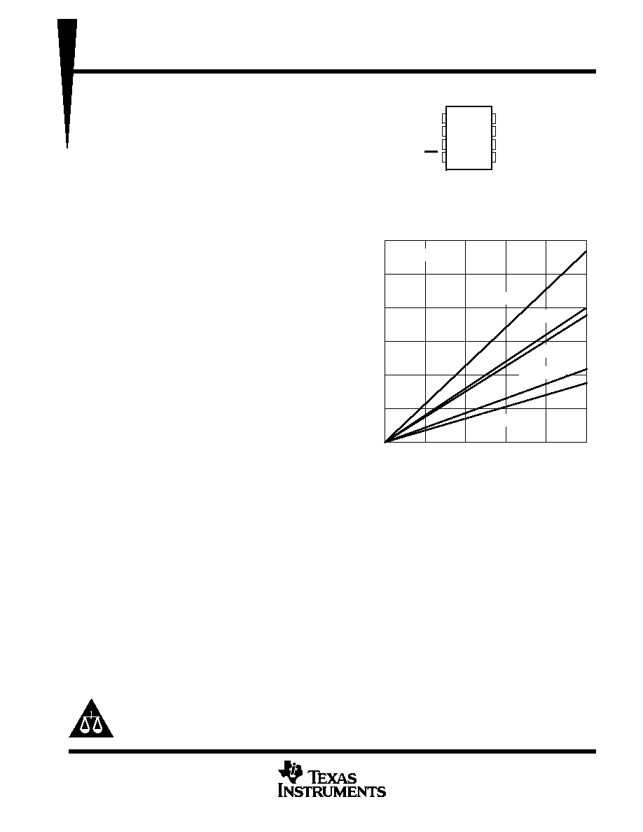
A combination of new circuit design and process
innovation has enabled the usual pnp pass
transistor to be replaced by a PMOS device.
Because the PMOS pass element behaves as a
low-value resistor, the dropout voltage is very low
≠ maximum of 85 mV at 100 mA of load current
(TPS7250) ≠ and is directly proportional to the
load current (see Figure 1). Since the PMOS pass
element is a voltage-driven device, the quiescent current is very low (300
µ
A maximum) and is stable over the
entire range of output load current (0 mA to 250 mA). Intended for use in portable systems such as laptops and
cellular phones, the low-dropout voltage and micropower operation result in a significant increase in system
battery operating life.
The TPS72xx also features a logic-enabled sleep mode to shut down the regulator, reducing quiescent current
to 0.5
µ
A maximum at T
J
= 25
∞
C. Other features include a power-good function that reports low output voltage
and may be used to implement a power-on reset or a low-battery indicator.
The TPS72xx is offered in 2.5-V, 2.75-V
ß
, 3-V, 3.3-V, 4.85-V, and 5-V fixed-voltage versions and in an adjustable
version (programmable over the range of 1.2 V to 9.75 V). Output voltage tolerance is specified as a maximum
of 2% over line, load, and temperature ranges (3% for adjustable version).
ß This device is in the product preview stage of development. Please contact the local TI sales office for availability.
Copyright
©
1998, Texas Instruments Incorporated
This document contains information on products in more than one phase
of development. The status of each device is indicated on the page(s)
specifying its electrical characteristics.
Please be aware that an important notice concerning availability, standard warranty, and use in critical applications of
Texas Instruments semiconductor products and disclaimers thereto appears at the end of this data sheet.
1
2
3
4
8
7
6
5
SENSE
/FB
RESET/PG
GND
EN
OUT
OUT
IN
IN
D, P, OR PW PACKAGE
(TOP VIEW)
SENSE ≠ Fixed voltage options only
(TPS7225, TPS7228
ß
, TPS7230, TPS7233,
TPS7248, and TPS7250)
FB ≠ Adjustable version only (TPS7201)
Figure 1. Typical Dropout Voltage Versus
Output Current
200
0
0
50
100
150
≠ Dropout V
oltage ≠ mV
400
200
250
100
300
V
DO
IO ≠ Output Current ≠ mA
TPS7233
TPS7248
TPS7250
TA = 25
∞
C
TPS7230
TPS7225
500
600
TPS7201Q, TPS7225Q, TPS7228Q, TPS7230Q
TPS7233Q, TPS7248Q, TPS7250Q, TPS72xxY
MICROPOWER LOW-DROPOUT (LDO) VOLTAGE REGULATORS
SLVS102F ≠ MARCH 1995 ≠ REVISED NOVEMBER 1998
2
POST OFFICE BOX 655303
∑
DALLAS, TEXAS 75265
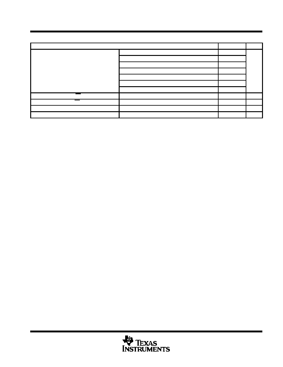
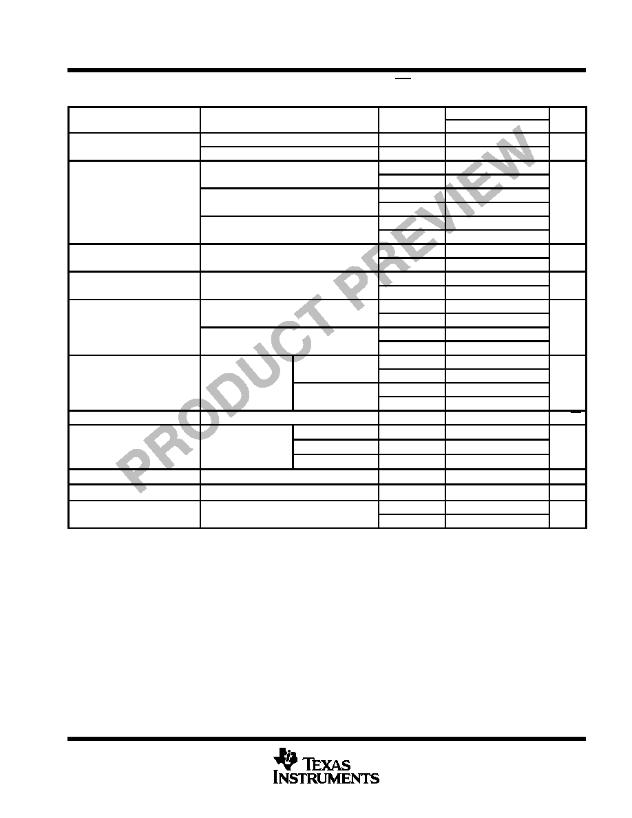
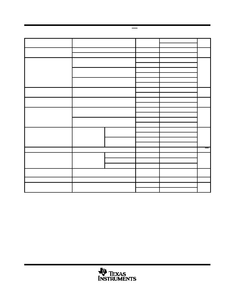
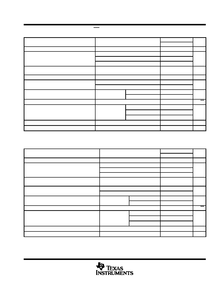
AVAILABLE OPTIONS
TJ
OUTPUT VOLTAGE
(V)
PACKAGED DEVICES
CHIP FORM
TJ
MIN
TYP
MAX
SMALL OUTLINE
(D)
PDIP
(P)
TSSOP
(PW)
(Y)
4.9
5
5.1
TPS7250QD
TPS7250QP
TPS7250QPWR
TPS7250Y
4.75
4.85
4.95
TPS7248QD
TPS7248QP
TPS7248QPWR
TPS7248Y
3.23
3.3
3.37
TPS7233QD
TPS7233QP
TPS7233QPWR
TPS7233Y
≠ 55
∞
C to 150
∞
C
2.94
3
3.06
TPS7230QD
TPS7230QP
TPS7230QPWR
TPS7230Y
≠ 55 C to 150 C
2.69
2.75
2.81
TPS7228QD
TPS7228QP
TPS7228QPWR
TPS7228Y
2.45
2.5
2.55
TPS7225QD
TPS7225QP
TPS7225QPWR
TPS7225Y
Adjustable
1.2 V to 9.75 V
TPS7201QD
TPS7201QP
TPS7201QPWR
TPS7201Y
The D package is available taped and reeled. Add R suffix to device type (e.g., TPS7250QDR). The PW package is only available left-end
taped and reeled. The TPS7201Q is programmable using an external resistor divider (see application information). The chip form is tested
at 25
∞
C.
TPS7225Q, TPS7228Q
, TPS7230Q, TPS7233Q, TPS7248Q, TPS7250Q
(fixed-voltage options)
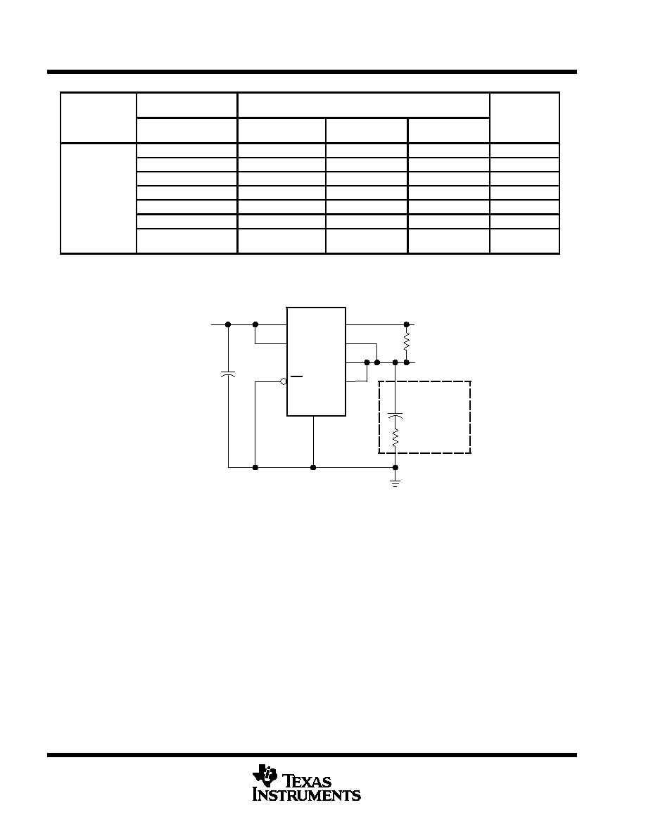
NOTE A: Capacitor selection is nontrivial. See application information section
for details.
SENSE
PG
OUT
OUT
6
5
4
IN
IN
EN
GND
3
2
1
7
8
VI
0.1
µ
F
PG
CSR = 1
VO
10
µ
F
+
TPS72xx
CO
(see Note A)
250 k
Figure 2. Typical Application Configuration
This device is in the product preview stage of development. Please contact the local TI sales office for availability.
TPS7201Q, TPS7225Q, TPS7228Q, TPS7230Q
TPS7233Q, TPS7248Q, TPS7250Q, TPS72xxY
MICROPOWER LOW-DROPOUT (LDO) VOLTAGE REGULATORS
SLVS102F ≠ MARCH 1995 ≠ REVISED NOVEMBER 1998
3
POST OFFICE BOX 655303
∑
DALLAS, TEXAS 75265
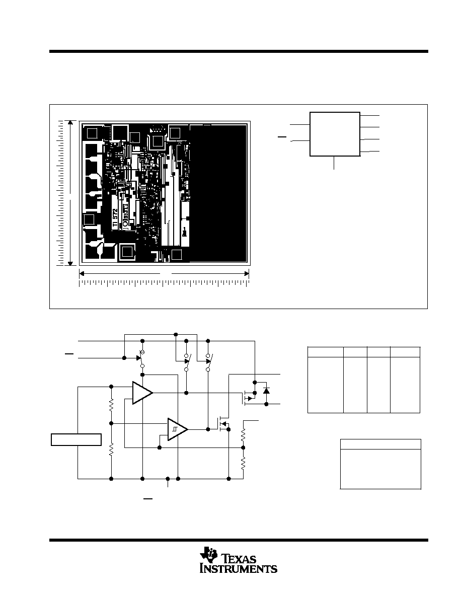
TPS72xx chip information
These chips, when properly assembled, display characteristics similar to the TPS72xxQ. Thermal compression
or ultrasonic bonding may be used on the doped aluminum bonding pads. The chips may be mounted with
conductive epoxy or a gold-silicon preform.
(6)
(4)
(3)
(7)
(2)
(1)
GND
FB
OUT
PG
IN
EN
TPS72xx
57
69
CHIP THICKNESS: 15 MILS TYPICAL
BONDING PADS: 4
◊
4 MILS MINIMUM
TJmax = 150
∞
C
TOLERANCES ARE
±
10%.
ALL DIMENSIONS ARE IN MILS.
(6)
(7)
(2)
(5)
(4)
(3)
(1)
BONDING PAD ASSIGNMENTS
SENSE
(5)
NOTE A. For most applications, OUT and SENSE should
be tied together as close as possible to the device;
for other implementations, refer to the SENSE-pin
connection discussion in the application
information section of this data sheet.
7
6
5
4
1
2
3
Fixed-voltage options only (TPS7225, TPS7228#,
TPS7230, TPS7233, TPS7248, and TPS7250)
Adjustable version only (TPS7201)
functional block diagram
_
+
Vref = 1.188 V
OUT
SENSE∂/FB
EN
IN
GND
R1
R2
PG
_
+
TPS7201
TPS7225
TPS7228#
TPS7230
TPS7233
TPS7248
TPS7250
DEVICE
UNIT
R1
R2
0
257
306
357
420
726
756
233
233
233
233
233
233
k
k
k
k
k
k
RESISTOR DIVIDER OPTIONS
ß Switch positions are shown with EN low (active).
∂ For most applications, SENSE should be externally connected to OUT as close as possible to the device.
For other implementations, refer to the SENSE-pin connection discussion in application information section.
NOTE A: Resistors are nominal values only.
1.12 V
ß
ß
ß
MOS transistors
Bilpolar transistors
Diodes
Capacitors
Resistors
COMPONENT COUNT
108
41
4
15
75
# This device is in the product preview stage of development. Please contact the local TI sales office for availability.
TPS7201Q, TPS7225Q, TPS7228Q, TPS7230Q
TPS7233Q, TPS7248Q, TPS7250Q, TPS72xxY
MICROPOWER LOW-DROPOUT (LDO) VOLTAGE REGULATORS
SLVS102F ≠ MARCH 1995 ≠ REVISED NOVEMBER 1998
4
POST OFFICE BOX 655303
∑
DALLAS, TEXAS 75265
absolute maximum ratings over operating free-air temperature range (unless otherwise noted)
Input voltage range , V
I
, PG, SENSE, EN
≠ 0.3 V to 11 V
. . . . . . . . . . . . . . . . . . . . . . . . . . . . . . . . . . . . . . . . . . . .
Output current, I
O
1.5 A
. . . . . . . . . . . . . . . . . . . . . . . . . . . . . . . . . . . . . . . . . . . . . . . . . . . . . . . . . . . . . . . . . . . . . . . . .
Continuous total power dissipation
See Dissipation Rating Tables 1 and 2
. . . . . . . . . . . . . . . . . . . . . . . . . . . . .
Operating virtual junction temperature range, T
J
≠ 55
∞
C to 150
∞
C
. . . . . . . . . . . . . . . . . . . . . . . . . . . . . . . . . . . . .
Storage temperature range, T
stg
≠ 65
∞
C to 150
∞
C
. . . . . . . . . . . . . . . . . . . . . . . . . . . . . . . . . . . . . . . . . . . . . . . . . . .
Lead temperature 1,6 mm (1/16 inch) from case for 10 seconds
260
∞
C
. . . . . . . . . . . . . . . . . . . . . . . . . . . . . . .
Stresses beyond those listed under "absolute maximum ratings" may cause permanent damage to the device. These are stress ratings only, and
functional operation of the device at these or any other conditions beyond those indicated under "recommended operating conditions" is not
implied. Exposure to absolute-maximum-rated conditions for extended periods may affect device reliability.
All voltage values are with respect to network ground terminal.
DISSIPATION RATING TABLE 1 ≠ FREE-AIR TEMPERATURE (see Note 1 and Figure 3)
PACKAGE
TA
25
∞
C
DERATING FACTOR
TA = 70
∞
C
TA = 85
∞
C
TA = 125
∞
C
PACKAGE
A
POWER RATING
ABOVE TA = 25
∞
C
A
POWER RATING
A
POWER RATING
A
POWER RATING
D
P
725 mW
1175 mW
5.8 mW/
∞
C
8 74 mW/
∞
C
464 mW
782 mW
377 mW
650 mW
145 mW
301 mW
P
PW
1175 mW
525 mW
8.74 mW/
∞
C
4.2 mW/
∞
C
782 mW
336 mW
650 mW
273 mW
301 mW
105 mW
DISSIPATION RATING TABLE 2 ≠ CASE TEMPERATURE (see Note 1 and Figure 4)
PACKAGE
TC
25
∞
C
DERATING FACTOR
TC = 70
∞
C
TC = 85
∞
C
TC = 125
∞
C
PACKAGE
C
POWER RATING
ABOVE TC = 25
∞
C
C
POWER RATING
C
POWER RATING
C
POWER RATING
D
P
2063 mW
2738 mW
16.5 mW/
∞
C
20 49 mW/
∞
C
1320 mW
1816 mW
1073 mW
1508 mW
413 mW
689 mW
P
PW
2738 mW
2900 mW
20.49 mW/
∞
C
23.2 mW/
∞
C
1816 mW
1856 mW
1508 mW
1508 mW
689 mW
580 mW
NOTE 1: Dissipation rating tables and figures are provided for maintenance of junction temperature at or below absolute
maximum of 150
∞
C. For guidelines on maintaining junction temperature within the recommended operating range,
see application information section.
Figure 3
600
400
200
0
25
50
75
100
800
1000
1200
125
150
1100
900
700
500
300
100
≠ Maximum Continuous Dissipation ≠ mW
MAXIMUM CONTINUOUS DISSIPATION
vs
FREE-AIR TEMPERATURE
P
D
TA ≠ Free-Air Temperature ≠
∞
C
D Package
R
JA = 172
∞
C/W
PW Package
R
JA = 238
∞
C/W
P Package
R
JA = 114.4
∞
C/W
Figure 4
≠ Maximum Continuous Dissipation ≠ mW
MAXIMUM CONTINUOUS DISSIPATION
vs
CASE TEMPERATURE
P
D
TC ≠ Case Temperature ≠
∞
C
1500
1000
500
0
25
50
75
100
2000
2500
3000
125
150
D Package
R
JC = 60.6
∞
C/W
PW Package
R
JC = 43.1
∞
C/W
P Package
R
JC = 48.8
∞
C/W
TPS7201Q, TPS7225Q, TPS7228Q, TPS7230Q
TPS7233Q, TPS7248Q, TPS7250Q, TPS72xxY
MICROPOWER LOW-DROPOUT (LDO) VOLTAGE REGULATORS
SLVS102F ≠ MARCH 1995 ≠ REVISED NOVEMBER 1998
5
POST OFFICE BOX 655303
∑
DALLAS, TEXAS 75265
recommended operating conditions
MIN
MAX
UNIT
TPS7201Q
3
10
TPS7225Q
3.65
10
TPS7228Q
TBD
10
Input voltage, VI
TPS7230Q
3.96
10
V
TPS7233Q
3.98
10
TPS7248Q
5.24
10
TPS7250Q
5.41
10
High-level input voltage at EN, VIH
2
V
Low-level input voltage at EN, VIL
0.5
V
Output current, IO
0
250
mA
Operating virtual junction temperature, TJ
≠ 40
125
∞
C
Minimum input voltage defined in the recommended operating conditions is the maximum specified output voltage plus dropout voltage at the
maximum specified load range. Since dropout voltage is a function of output current, the usable range can be extended for lighter loads. To
calculate the minimum input voltage for the maximum load current used in a given application, use the following equation:
V
I(min)
+
V
O(max)
)
V
DO(max load)
Because the TPS7201 is programmable, rDS(on) should be used to calculate VDO before applying the above equation. The equation for
calculating VDO from rDS(on) is given in Note 3 under the TPS7201 electrical characteristics table. The minimum value of 3 V is the absolute
lower limit for the recommended input-voltage range for the TPS7201.
This device is in the product preview stage of development. Please contact the local TI sales office for availability.
TPS7201Q, TPS7225Q, TPS7228Q, TPS7230Q
TPS7233Q, TPS7248Q, TPS7250Q, TPS72xxY
MICROPOWER LOW-DROPOUT (LDO) VOLTAGE REGULATORS
SLVS102F ≠ MARCH 1995 ≠ REVISED NOVEMBER 1998
6
POST OFFICE BOX 655303
∑
DALLAS, TEXAS 75265
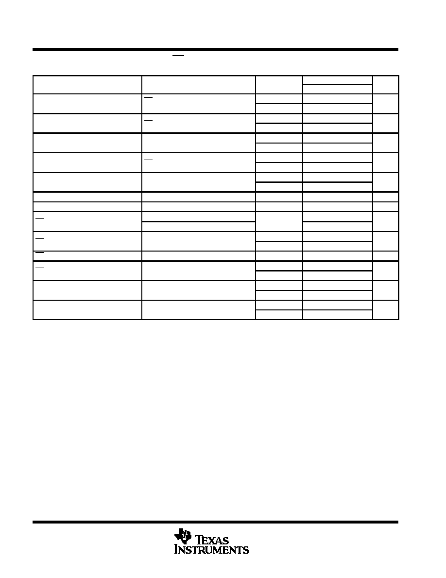
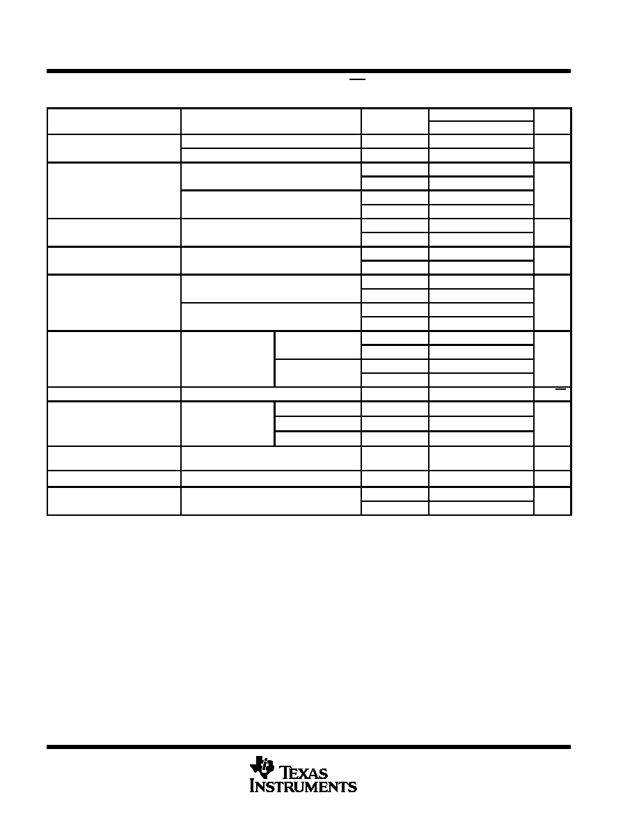
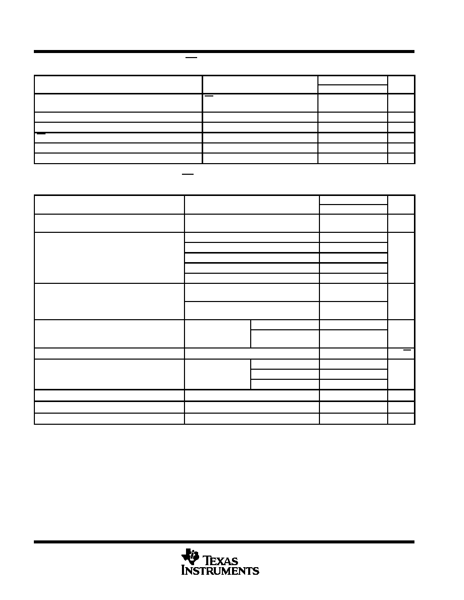
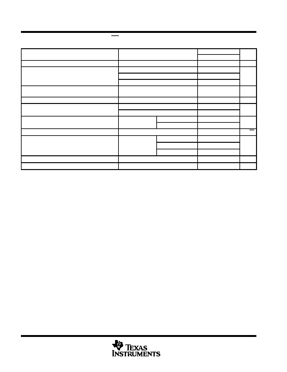
electrical characteristics, I
O
= 10 mA, EN = 0 V, C
O
= 4.7
µ
F (CSR
= 1
), SENSE/FB shorted to OUT
(unless otherwise noted)
PARAMETER
TEST CONDITIONS
TJ
TPS72xxQ
UNIT
PARAMETER
TEST CONDITIONS
TJ
MIN
TYP
MAX
UNIT
Ground current (active mode)
EN
0.5 V,
VI = VO + 1 V,
25
∞
C
180
225
µ
A
Ground current (active mode)
EN
0.5 V,
0 mA
IO
250 mA
VI VO + 1 V,
≠ 40
∞
C to 125
∞
C
325
µ
A
Input current (standby mode)
EN
V
3 V
V
10 V
25
∞
C
0.5
µ
A
Input current (standby mode)
EN = VI,
3 V
VI
10 V
≠ 40
∞
C to 125
∞
C
1
µ
A
Output current limit threshold
VO = 0 V
VI = 10 V
25
∞
C
0.6
1
A
Output current limit threshold
VO = 0 V
VI = 10 V
≠ 40
∞
C to 125
∞
C
1.5
A
Pass-element leakage current in
EN
VI
3 V
VI
10 V
25
∞
C
0.5
µ
A
g
standby mode
EN = VI,
3 V
VI
10 V
≠ 40
∞
C to 125
∞
C
1
µ
A
PG leakage current
VPG = 10 V
Normal operation
25
∞
C
0.5
µ
A
PG leakage current
VPG = 10 V,
Normal operation
≠ 40
∞
C to 125
∞
C
0.5
µ
A
Output voltage temperature coefficient
≠ 40
∞
C to 125
∞
C
31
75
ppm/
∞
C
Thermal shutdown junction temperature
165
∞
C
EN logic high (standby mode)
3 V
VI
6 V
40
∞
C to 125
∞
C
2
V
EN logic high (standby mode)
6 V
VI
10 V
≠ 40
∞
C to 125
∞
C
2.7
V
EN logic low (active mode)
3 V
VI
10 V
25
∞
C
0.5
V
EN logic low (active mode)
3 V
VI
10 V
≠ 40
∞
C to 125
∞
C
0.5
V
EN hysteresis voltage
25
∞
C
50
mV
EN input current
0 V
VI
10 V
25
∞
C
≠ 0.5
0.5
µ
A
EN input current
0 V
VI
10 V
≠ 40
∞
C to 125
∞
C
≠ 0.5
0.5
µ
A
Minimum VI for active pass element
25
∞
C
1.9
2.5
V
Minimum VI for active pass element
≠ 40
∞
C to 125
∞
C
2.5
V
Minimum VI for valid PG
IPG = 300
µ
A
25
∞
C
1.1
1.5
V
Minimum VI for valid PG
IPG = 300
µ
A
≠ 40
∞
C to 125
∞
C
1.9
V
CSR(compensation series resistance) refers to the total series resistance, including the equivalent series resistance (ESR) of the capacitor, any
series resistance added externally, and PWB trace resistance to CO.
Pulse-testing techniques are used to maintain virtual junction temperature as close as possible to ambient temperature; thermal effects must
be taken into account separately.
TPS7201Q, TPS7225Q, TPS7228Q, TPS7230Q
TPS7233Q, TPS7248Q, TPS7250Q, TPS72xxY
MICROPOWER LOW-DROPOUT (LDO) VOLTAGE REGULATORS
SLVS102F ≠ MARCH 1995 ≠ REVISED NOVEMBER 1998
7
POST OFFICE BOX 655303
∑
DALLAS, TEXAS 75265
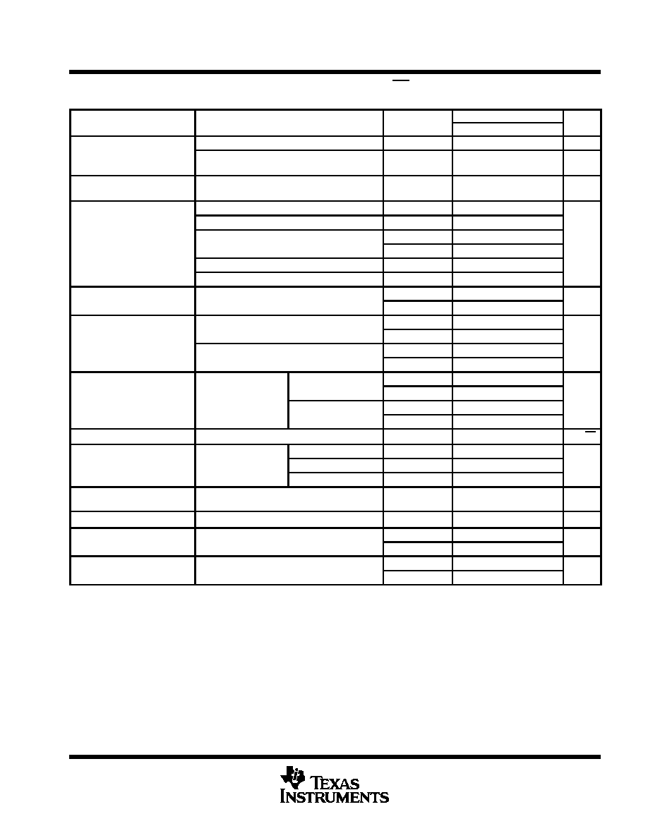
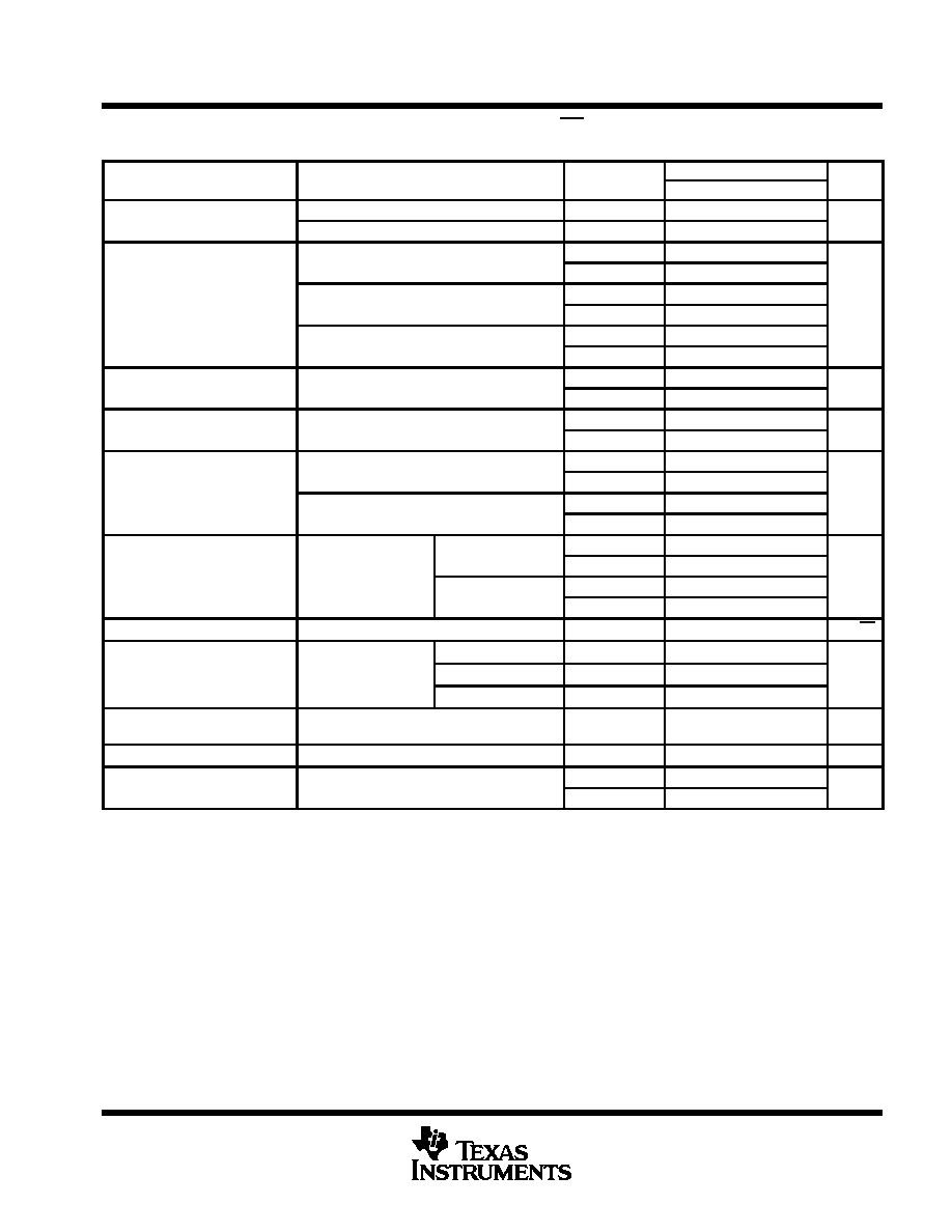
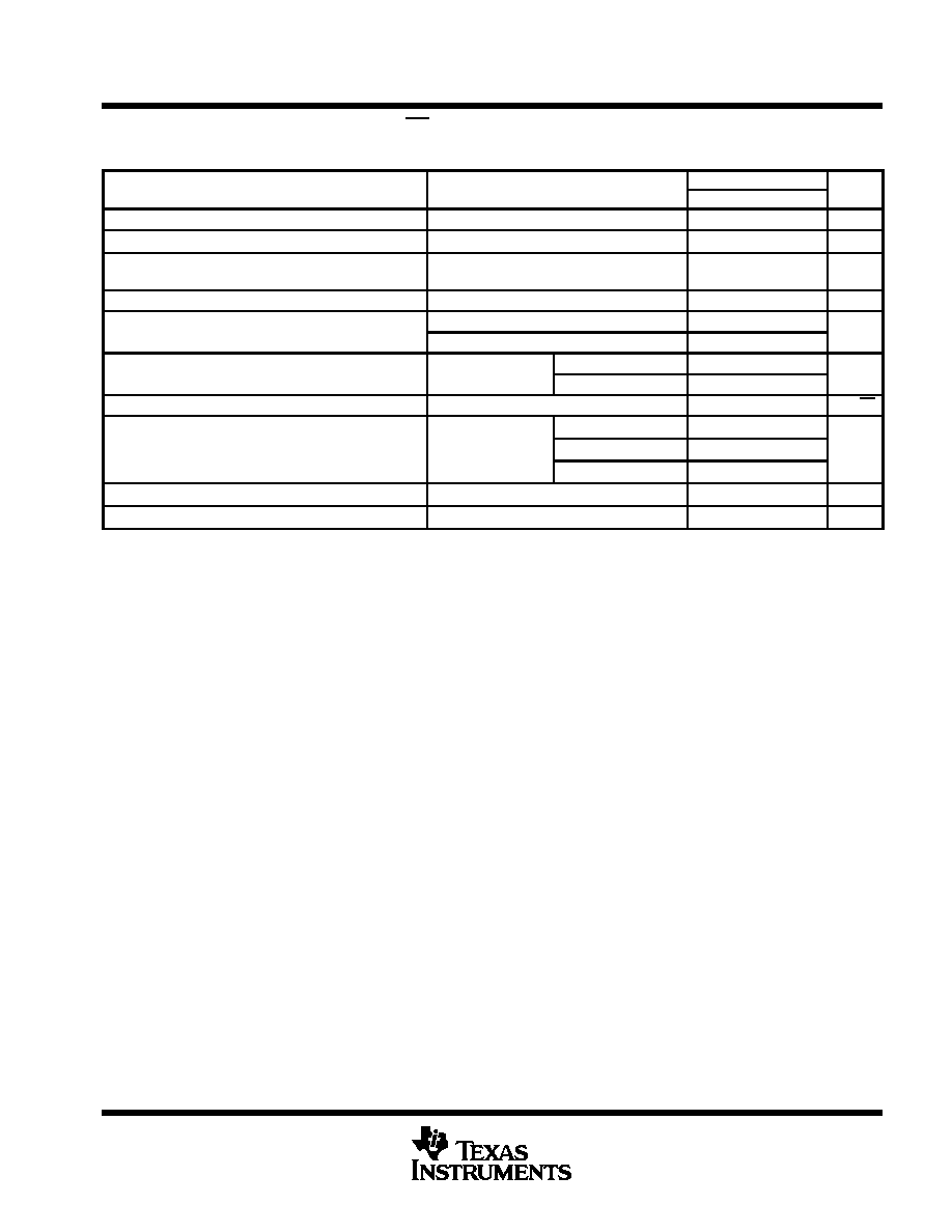
TPS7201Q electrical characteristics, I
O
= 10 mA, V
I
= 3.5 V, EN = 0 V, C
O
= 4.7
µ
F (CSR
= 1
), FB
shorted to OUT at device leads (unless otherwise noted)
PARAMETER
TEST CONDITIONS
TJ
TPS7201Q
UNIT
PARAMETER
TEST CONDITIONS
TJ
MIN
TYP
MAX
UNIT
Reference voltage (measured
VI = 3.5 V,
IO = 10 mA
25
∞
C
1.188
V
g (
at FB with OUT connected to
FB)
3 V
VI
10 V,
See Note 2
5 mA
IO
250 mA,
≠ 40
∞
C to 125
∞
C
1.152
1.224
V
Reference voltage
temperature coefficient
≠ 40
∞
C to 125
∞
C
31
75
ppm/
∞
C
VI = 2.4 V,ß
50
µ
A
IO
100 mA
25
∞
C
2.1
VI = 2.4 V,ß
100 mA
IO
200 mA
25
∞
C
2.9
Pass-element series
VI = 2 9 V
50
µ
A
IO
250 mA
25
∞
C
1.6
2.7
resistance (see Note 3)
VI = 2.9 V,
50
µ
A
IO
250 mA
≠ 40
∞
C to 125
∞
C
4.5
VI = 3.9 V,
50
µ
A
IO
250 mA
25
∞
C
1
VI = 5.9 V,
50
µ
A
IO
250 mA
25
∞
C
0.8
Input regulation
VI = 3 V to 10 V,
50
µ
A
IO
250 mA,
25
∞
C
23
mV
Input regulation
I
,
See Note 2
µ
O
,
≠ 40
∞
C to 125
∞
C
36
mV
IO = 5 mA to 250 mA,
3 V
VI
10 V,
25
∞
C
15
25
Output regulation
O
,
See Note 2
I
,
≠ 40
∞
C to 125
∞
C
36
mV
Output regulation
IO = 50
µ
A to 250 mA,
3 V
VI
10 V,
25
∞
C
17
27
mV
O
µ
,
See Note 2
I
,
≠ 40
∞
C to 125
∞
C
43
IO = 50
µ
A
25
∞
C
49
60
Ripple rejection
f = 120 Hz
IO = 50
µ
A
≠ 40
∞
C to 125
∞
C
32
dB
Ripple rejection
f = 120 Hz
IO = 250 mA,
25
∞
C
45
50
dB
O
,
See Note 2
≠ 40
∞
C to 125
∞
C
30
Output noise spectral density
f = 120 Hz
25
∞
C
2
µ
V/
Hz
10 H
f
100 kH
CO = 4.7
µ
F
25
∞
C
235
Output noise voltage
10 Hz
f
100 kHz,
CSR = 1
CO = 10
µ
F
25
∞
C
190
µ
Vrms
CSR = 1
CO = 100
µ
F
25
∞
C
125
PG trip-threshold voltage∂
VFB voltage decreasing from above VPG
≠ 40
∞
C to 125
∞
C
0.95
◊
VFB(nom)
V
PG hysteresis voltage∂
Measured at VFB
25
∞
C
12
mV
PG output low voltage∂
IPG = 400
µ
A
VI = 2 13 V
25
∞
C
0.1
0.4
V
PG output low voltage∂
IPG = 400
µ
A,
VI = 2.13 V
≠ 40
∞
C to 125
∞
C
0.4
V
FB input current
25
∞
C
≠ 10
0.1
10
nA
FB input current
≠ 40
∞
C to 125
∞
C
≠ 20
20
nA
CSR refers to the total series resistance, including the ESR of the capacitor, any series resistance added externally, and PWB trace resistance
to CO.
Pulse-testing techniques are used to maintain virtual junction temperature as close as possible to ambient temperature; thermal effects must
be taken into account separately.
ß This voltage is not recommended.
∂ Output voltage programmed to 2.5 V with closed-loop configuration (see application information).
NOTES:
2. When VI < 2.9 V and IO > 100 mA simultaneously, pass element rDS(on) increases (see Figure 10) to a point such that the resulting
dropout voltage prevents the regulator from maintaining the specified tolerance range.
3. To calculate dropout voltage, use equation:
VDO = IO
rDS(on)
rDS(on) is a function of both output current and input voltage. The parametric table lists rDS(on) for VI = 2.4 V, 2.9 V, 3.9 V, and
5.9 V, which corresponds to dropout conditions for programmed output voltages of 2.5 V, 3 V, 4 V, and 6 V, respectively. For other
programmed values, refer to Figures 10 and 11.
TPS7201Q, TPS7225Q, TPS7228Q, TPS7230Q
TPS7233Q, TPS7248Q, TPS7250Q, TPS72xxY
MICROPOWER LOW-DROPOUT (LDO) VOLTAGE REGULATORS
SLVS102F ≠ MARCH 1995 ≠ REVISED NOVEMBER 1998
8
POST OFFICE BOX 655303
∑
DALLAS, TEXAS 75265
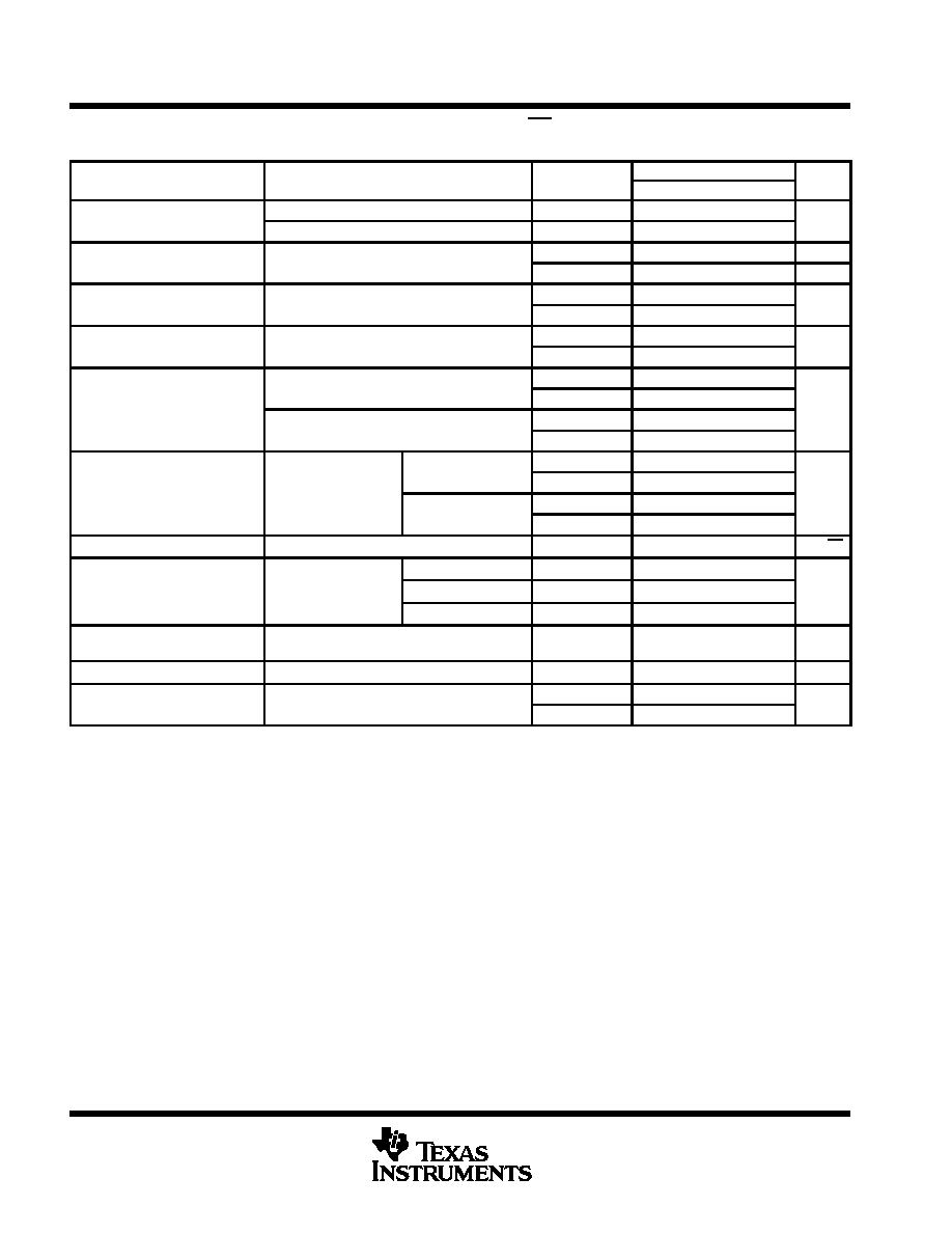
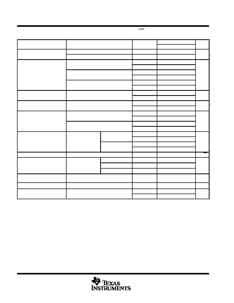
TPS7225Q electrical characteristics, I
O
= 10 mA, V
I
= 3.5 V, EN = 0 V, C
O
= 4.7
µ
F (CSR
= 1
), SENSE
shorted to OUT (unless otherwise noted)
PARAMETER
TEST CONDITIONS
TJ
TPS7225Q
UNIT
PARAMETER
TEST CONDITIONS
TJ
MIN
TYP
MAX
UNIT
Output voltage
VI = 3.5 V,
IO = 10 mA
25
∞
C
2.5
V
Output voltage
3.5 V
VI
10 V,
5 mA
IO
250 mA
≠ 40
∞
C to 125
∞
C
2.45
2.55
V
Dropout voltage
IO = 250 mA
VI = 2 97 V
25
∞
C
560
850
mV
Dropout voltage
IO = 250 mA,
VI = 2.97 V
≠ 40
∞
C to 125
∞
C
1.1
V
Pass element series resistance
(2.97 V ≠ VO)/IO,
VI = 2.97 V,
25
∞
C
2.24
3.4
Pass-element series resistance
(
O) O,
IO = 250 mA
I
,
≠ 40
∞
C to 125
∞
C
3.84
Input regulation
VI = 3 5 V to 10 V
50
µ
A
IO
250 mA
25
∞
C
9
27
mV
Input regulation
VI = 3.5 V to 10 V,
50
µ
A
IO
250 mA
≠ 40
∞
C to 125
∞
C
33
mV
IO = 5 mA to 250 mA
3 5 V
VI
10 V
25
∞
C
28
36
Output regulation
IO = 5 mA to 250 mA,
3.5 V
VI
10 V
≠ 40
∞
C to 125
∞
C
60
mV
Output regulation
IO = 50
µ
A to 250 mA
3 5 V
VI
10 V
25
∞
C
24
41
mV
IO = 50
µ
A to 250 mA,
3.5 V
VI
10 V
≠ 40
∞
C to 125
∞
C
73
IO = 50
µ
A
25
∞
C
47
58
Ripple rejection
f = 120 Hz
IO = 50
µ
A
≠ 40
∞
C to 125
∞
C
45
dB
Ripple rejection
f = 120 Hz
IO = 250 mA
25
∞
C
40
46
dB
IO = 250 mA
≠ 40
∞
C to 125
∞
C
38
Output noise spectral density
f = 120 Hz
25
∞
C
2
µ
V/
Hz
10 H
f
100 kH
CO = 4.7
µ
F
25
∞
C
248
Output noise voltage
10 Hz
f
100 kHz,
CSR = 1
CO = 10
µ
F
25
∞
C
200
µ
Vrms
CSR = 1
CO = 100
µ
F
25
∞
C
130
PG trip-threshold voltage
VO voltage decreasing from above VPG
≠ 40
∞
C to 125
∞
C
0.95
◊
VO(nom)
V
PG hysteresis voltage
25
∞
C
50
mV
PG output low voltage
IPG = 1 2 mA
VI = 2 13 V
25
∞
C
0.3
0.44
V
PG output low voltage
IPG = 1.2 mA,
VI = 2.13 V
≠ 40
∞
C to 125
∞
C
0.5
V
CSR refers to the total series resistance, including the ESR of the capacitor, any series resistance added externally, and PWB trace resistance
to CO.
Pulse-testing techniques are used to maintain virtual junction temperature as close as possible to ambient temperature; thermal effects must
be taken into account separately.
TPS7201Q, TPS7225Q, TPS7228Q, TPS7230Q
TPS7233Q, TPS7248Q, TPS7250Q, TPS72xxY
MICROPOWER LOW-DROPOUT (LDO) VOLTAGE REGULATORS
SLVS102F ≠ MARCH 1995 ≠ REVISED NOVEMBER 1998
9
POST OFFICE BOX 655303
∑
DALLAS, TEXAS 75265
TPS7228Q electrical characteristics, I
O
= 10 mA, V
I
= 3.75 V, EN = 0 V, C
O
= 4.7
µ
F (CSR
= 1
),
SENSE shorted to OUT (unless otherwise noted)
PARAMETER
TEST CONDITIONS
TJ
TPS7228Q
UNIT
PARAMETER
TEST CONDITIONS
TJ
MIN
TYP
MAX
UNIT
Output voltage
VI = 3.75 V,
IO = 10 mA
25
∞
C
2.75
V
Output voltage
3.75 V
VI
10 V,
5 mA
IO
250 mA
≠ 40
∞
C to 125
∞
C
2.69
2.81
V
IO = 10 mA
VI = 2 69 V
25
∞
C
TBD
IO = 10 mA,
VI = 2.69 V
≠ 40
∞
C to 125
∞
C
TBD
Dropout voltage
IO = 100 mA
VI = 2 69 V
25
∞
C
TBD
mV
Dropout voltage
IO = 100 mA,
VI = 2.69 V
≠ 40
∞
C to 125
∞
C
TBD
mV
IO = 250 mA
VI = 2 69 V
25
∞
C
TBD
IO = 250 mA,
VI = 2.69 V
≠ 40
∞
C to 125
∞
C
TBD
Pass element series resistance
(2.69 V ≠ VO)/IO,
VI = 2.69 V,
25
∞
C
TBD
Pass-element series resistance
(
O) O,
IO = 250 mA
I
,
≠ 40
∞
C to 125
∞
C
TBD
Input regulation
VI = 3 75 V to 10 V
50
µ
A
IO
250 mA
25
∞
C
TBD
mV
Input regulation
VI = 3.75 V to 10 V,
50
µ
A
IO
250 mA
≠ 40
∞
C to 125
∞
C
TBD
mV
IO = 5 mA to 250 mA
3 75 V
VI
10 V
25
∞
C
TBD
Output regulation
IO = 5 mA to 250 mA,
3.75 V
VI
10 V
≠ 40
∞
C to 125
∞
C
TBD
mV
Output regulation
IO = 50
µ
A to 250 mA
3 75 V
VI
10 V
25
∞
C
TBD
mV
IO = 50
µ
A to 250 mA,
3.75 V
VI
10 V
≠ 40
∞
C to 125
∞
C
TBD
IO = 50
µ
A
25
∞
C
TBD
Ripple rejection
f = 120 Hz
IO = 50
µ
A
≠ 40
∞
C to 125
∞
C
TBD
dB
Ripple rejection
f = 120 Hz
IO = 250 mA
25
∞
C
TBD
dB
IO = 250 mA
≠ 40
∞
C to 125
∞
C
TBD
Output noise spectral density
f = 120 Hz
25
∞
C
TBD
µ
V/
Hz
10 H
f
100 kH
CO = 4.7
µ
F
25
∞
C
TBD
Output noise voltage
10 Hz
f
100 kHz,
CSR = 1
CO = 10
µ
F
25
∞
C
TBD
µ
Vrms
CSR = 1
CO = 100
µ
F
25
∞
C
TBD
PG trip-threshold voltage
VO voltage decreasing from above VPG
≠ 40
∞
C to 125
∞
C
TBD
V
PG hysteresis voltage
25
∞
C
TBD
mV
PG output low voltage
IPG = 1 2 mA
VI = 2 34 V
25
∞
C
TBD
V
PG output low voltage
IPG = 1.2 mA,
VI = 2.34 V
≠ 40
∞
C to 125
∞
C
TBD
V
CSR refers to the total series resistance, including the ESR of the capacitor, any series resistance added externally, and PWB trace resistance
to CO.
Pulse-testing techniques are used to maintain virtual junction temperature as close as possible to ambient temperature; thermal effects must
be taken into account separately.
TPS7201Q, TPS7225Q, TPS7228Q, TPS7230Q
TPS7233Q, TPS7248Q, TPS7250Q, TPS72xxY
MICROPOWER LOW-DROPOUT (LDO) VOLTAGE REGULATORS
SLVS102F ≠ MARCH 1995 ≠ REVISED NOVEMBER 1998
10
POST OFFICE BOX 655303
∑
DALLAS, TEXAS 75265
TPS7230Q electrical characteristics, I
O
= 10 mA, V
I
= 4 V, EN = 0 V, C
O
= 4.7
µ
F (CSR
= 1
), SENSE
shorted to OUT (unless otherwise noted)
PARAMETER
TEST CONDITIONS
TJ
TPS7230Q
UNIT
PARAMETER
TEST CONDITIONS
TJ
MIN
TYP
MAX
UNIT
Output voltage
VI = 4 V,
IO = 10 mA
25
∞
C
3
V
Output voltage
4 V
VI
10 V,
5 mA
IO
250 mA
≠ 40
∞
C to 125
∞
C
2.94
3.06
V
IO = 100 mA
VI = 2 97 V
25
∞
C
145
185
Dropout voltage
IO = 100 mA,
VI = 2.97 V
≠ 40
∞
C to 125
∞
C
270
mV
Dropout voltage
IO = 250 mA
VI = 2 97 V
25
∞
C
390
502
mV
IO = 250 mA,
VI = 2.97 V
≠ 40
∞
C to 125
∞
C
900
Pass element series resistance
(2.97 V ≠ VO)/IO,
VI = 2.97 V,
25
∞
C
1.56
2.01
Pass-element series resistance
(
O) O,
IO = 250 mA
I
,
≠ 40
∞
C to 125
∞
C
3.6
Input regulation
VI = 4 V to 10 V
50
µ
A
IO
250 mA
25
∞
C
9
27
mV
Input regulation
VI = 4 V to 10 V,
50
µ
A
IO
250 mA
≠ 40
∞
C to 125
∞
C
33
mV
IO = 5 mA to 250 mA
4 V
VI
10 V
25
∞
C
34
45
Output regulation
IO = 5 mA to 250 mA,
4 V
VI
10 V
≠ 40
∞
C to 125
∞
C
74
mV
Output regulation
IO = 50
µ
A to 250 mA
4 V
VI
10 V
25
∞
C
42
60
mV
IO = 50
µ
A to 250 mA,
4 V
VI
10 V
≠ 40
∞
C to 125
∞
C
98
IO = 50
µ
A
25
∞
C
45
56
Ripple rejection
f = 120 Hz
IO = 50
µ
A
≠ 40
∞
C to 125
∞
C
44
dB
Ripple rejection
f = 120 Hz
IO = 250 mA
25
∞
C
40
45
dB
IO = 250 mA
≠ 40
∞
C to 125
∞
C
38
Output noise spectral density
f = 120 Hz
25
∞
C
2
µ
V/
Hz
10 H
f
100 kH
CO = 4.7
µ
F
25
∞
C
256
Output noise voltage
10 Hz
f
100 kHz,
CSR = 1
CO = 10
µ
F
25
∞
C
206
µ
Vrms
CSR = 1
CO = 100
µ
F
25
∞
C
132
PG trip-threshold voltage
VO voltage decreasing from above VPG
≠ 40
∞
C to 125
∞
C
0.95
◊
VO(nom)
V
PG hysteresis voltage
25
∞
C
50
mV
PG output low voltage
IPG = 1 2 mA
VI = 2 55 V
25
∞
C
0.25
0.44
V
PG output low voltage
IPG = 1.2 mA,
VI = 2.55 V
≠ 40
∞
C to 125
∞
C
0.44
V
CSR refers to the total series resistance, including the ESR of the capacitor, any series resistance added externally, and PWB trace resistance
to CO.
Pulse-testing techniques are used to maintain virtual junction temperature as close as possible to ambient temperature; thermal effects must
be taken into account separately.
TPS7201Q, TPS7225Q, TPS7228Q, TPS7230Q
TPS7233Q, TPS7248Q, TPS7250Q, TPS72xxY
MICROPOWER LOW-DROPOUT (LDO) VOLTAGE REGULATORS
SLVS102F ≠ MARCH 1995 ≠ REVISED NOVEMBER 1998
11
POST OFFICE BOX 655303
∑
DALLAS, TEXAS 75265
TPS7233Q electrical characteristics, I
O
= 10 mA, V
I
= 4.3 V, EN = 0 V, C
O
= 4.7
µ
F (CSR
= 1
), SENSE
shorted to OUT (unless otherwise noted)
PARAMETER
TEST CONDITIONS
TJ
TPS7233Q
UNIT
PARAMETER
TEST CONDITIONS
TJ
MIN
TYP
MAX
UNIT
Output voltage
VI = 4.3 V,
IO = 10 mA
25
∞
C
3.3
V
Output voltage
4.3 V
VI
10 V,
5 mA
IO
250 mA
≠ 40
∞
C to 125
∞
C
3.23
3.37
V
IO = 10 mA
VI = 3 23 V
25
∞
C
14
20
IO = 10 mA,
VI = 3.23 V
≠ 40
∞
C to 125
∞
C
30
Dropout voltage
IO = 100 mA
VI = 3 23 V
25
∞
C
140
180
mV
Dropout voltage
IO = 100 mA,
VI = 3.23 V
≠ 40
∞
C to 125
∞
C
232
mV
IO = 250 mA
VI = 3 23 V
25
∞
C
360
460
IO = 250 mA,
VI = 3.23 V
≠ 40
∞
C to 125
∞
C
610
Pass element series resistance
(3.23 V ≠ VO)/IO,
VI = 3.23 V,
25
∞
C
1.5
1.84
Pass-element series resistance
(
O) O,
IO = 250 mA
I
,
≠ 40
∞
C to 125
∞
C
2.5
Input regulation
VI = 4 3 V to 10 V
50
µ
A
IO
250 mA
25
∞
C
8
25
mV
Input regulation
VI = 4.3 V to 10 V,
50
µ
A
IO
250 mA
≠ 40
∞
C to 125
∞
C
33
mV
IO = 5 mA to 250 mA
4 3 V
VI
10 V
25
∞
C
32
42
Output regulation
IO = 5 mA to 250 mA,
4.3 V
VI
10 V
≠ 40
∞
C to 125
∞
C
71
mV
Output regulation
IO = 50
µ
A to 250 mA
4 3 V
VI
10 V
25
∞
C
41
55
mV
IO = 50
µ
A to 250 mA,
4.3 V
VI
10 V
≠ 40
∞
C to 125
∞
C
98
IO = 50
µ
A
25
∞
C
40
52
Ripple rejection
f = 120 Hz
IO = 50
µ
A
≠ 40
∞
C to 125
∞
C
38
dB
Ripple rejection
f = 120 Hz
IO = 250 mA
25
∞
C
35
44
dB
IO = 250 mA
≠ 40
∞
C to 125
∞
C
33
Output noise spectral density
f = 120 Hz
25
∞
C
2
µ
V/
Hz
10 H
f
100 kH
CO = 4.7
µ
F
25
∞
C
265
Output noise voltage
10 Hz
f
100 kHz,
CSR = 1
CO = 10
µ
F
25
∞
C
212
µ
Vrms
CSR = 1
CO = 100
µ
F
25
∞
C
135
PG trip-threshold voltage
VO voltage decreasing from above VPG
≠ 40
∞
C to 125
∞
C
0.95
◊
VO(nom)
V
PG hysteresis voltage
25
∞
C
32
mV
PG output low voltage
IPG = 1 2 mA
VI = 2 8 V
25
∞
C
0.22
0.4
V
PG output low voltage
IPG = 1.2 mA,
VI = 2.8 V
≠ 40
∞
C to 125
∞
C
0.4
V
CSR refers to the total series resistance, including the ESR of the capacitor, any series resistance added externally, and PWB trace resistance
to CO.
Pulse-testing techniques are used to maintain virtual junction temperature as close as possible to ambient temperature; thermal effects must
be taken into account separately.
TPS7201Q, TPS7225Q, TPS7228Q, TPS7230Q
TPS7233Q, TPS7248Q, TPS7250Q, TPS72xxY
MICROPOWER LOW-DROPOUT (LDO) VOLTAGE REGULATORS
SLVS102F ≠ MARCH 1995 ≠ REVISED NOVEMBER 1998
12
POST OFFICE BOX 655303
∑
DALLAS, TEXAS 75265
TPS7248Q electrical characteristics, I
O
= 10 mA, V
I
= 5.85 V, EN = 0 V, C
O
= 4.7
µ
F (CSR
= 1
),
SENSE shorted to OUT (unless otherwise noted)
PARAMETER
TEST CONDITIONS
TJ
TPS7248Q
UNIT
PARAMETER
TEST CONDITIONS
TJ
MIN
TYP
MAX
UNIT
Output voltage
VI = 5.85 V,
IO = 10 mA
25
∞
C
4.85
V
Output voltage
5.85 V
VI
10 V,
5 mA
IO
250 mA
≠ 40
∞
C to 125
∞
C
4.75
4.95
V
IO = 10 mA
VI = 4 75 V
25
∞
C
10
19
IO = 10 mA,
VI = 4.75 V
≠ 40
∞
C to 125
∞
C
30
Dropout voltage
IO = 100 mA
VI = 4 75 V
25
∞
C
90
100
mV
Dropout voltage
IO = 100 mA,
VI = 4.75 V
≠ 40
∞
C to 125
∞
C
150
mV
IO = 250 mA
VI = 4 75 V
25
∞
C
216
250
IO = 250 mA,
VI = 4.75 V
≠ 40
∞
C to 125
∞
C
285
Pass element series resistance
(4.75 V ≠ VO)/IO,
VI = 4.75 V,
25
∞
C
0.8
1
Pass-element series resistance
(
O) O,
IO = 250 mA
I
,
≠ 40
∞
C to 125
∞
C
1.4
Input regulation
VI = 5 85 V to 10 V
50
µ
A
IO
250 mA
25
∞
C
34
mV
Input regulation
VI = 5.85 V to 10 V,
50
µ
A
IO
250 mA
≠ 40
∞
C to 125
∞
C
50
mV
IO = 5 mA to 250 mA
5 85 V
VI
10 V
25
∞
C
43
55
Output regulation
IO = 5 mA to 250 mA,
5.85 V
VI
10 V
≠ 40
∞
C to 125
∞
C
95
mV
Output regulation
IO = 50
µ
A to 250 mA
5 85 V
VI
10 V
25
∞
C
55
75
mV
IO = 50
µ
A to 250 mA,
5.85 V
VI
10 V
≠ 40
∞
C to 125
∞
C
135
IO = 50
µ
A
25
∞
C
42
53
Ripple rejection
f = 120 Hz
IO = 50
µ
A
≠ 40
∞
C to 125
∞
C
36
dB
Ripple rejection
f = 120 Hz
IO = 250 mA
25
∞
C
36
46
dB
IO = 250 mA
≠ 40
∞
C to 125
∞
C
34
Output noise spectral density
f = 120 Hz
25
∞
C
2
µ
V/
Hz
10 H
f
100 kH
CO = 4.7
µ
F
25
∞
C
370
Output noise voltage
10 Hz
f
100 kHz,
CSR = 1
CO = 10
µ
F
25
∞
C
290
µ
Vrms
CSR = 1
CO = 100
µ
F
25
∞
C
168
PG trip-threshold voltage
VO voltage decreasing from above VPG
≠ 40
∞
C to 125
∞
C
0.95
◊
VO(nom)
V
PG hysteresis voltage
25
∞
C
50
mV
PG output low voltage
IPG = 1 2 mA
VI = 4 12 V
25
∞
C
0.2
0.4
V
PG output low voltage
IPG = 1.2 mA,
VI = 4.12 V
≠ 40
∞
C to 125
∞
C
0.4
V
CSR refers to the total series resistance, including the ESR of the capacitor, any series resistance added externally, and PWB trace resistance
to CO.
Pulse-testing techniques are used to maintain virtual junction temperature as close as possible to ambient temperature; thermal effects must
be taken into account separately.
TPS7201Q, TPS7225Q, TPS7228Q, TPS7230Q
TPS7233Q, TPS7248Q, TPS7250Q, TPS72xxY
MICROPOWER LOW-DROPOUT (LDO) VOLTAGE REGULATORS
SLVS102F ≠ MARCH 1995 ≠ REVISED NOVEMBER 1998
13
POST OFFICE BOX 655303
∑
DALLAS, TEXAS 75265
TPS7250Q electrical characteristics, I
O
= 10 mA, V
I
= 6 V, EN = 0 V, C
O
= 4.7
µ
F (CSR
= 1
), SENSE
shorted to OUT (unless otherwise noted)
PARAMETER
TEST CONDITIONS
TJ
TPS7250Q
UNIT
PARAMETER
TEST CONDITIONS
TJ
MIN
TYP
MAX
UNIT
Output voltage
VI = 6 V,
IO = 10 mA
25
∞
C
5
V
Output voltage
6 V
VI
10 V,
5 mA
IO
250 mA
≠ 40
∞
C to 125
∞
C
4.9
5.1
V
IO = 10 mA
VI = 4 88 V
25
∞
C
8
12
IO = 10 mA,
VI = 4.88 V
≠ 40
∞
C to 125
∞
C
30
Dropout voltage
IO = 100 mA
VI = 4 88 V
25
∞
C
76
85
mV
Dropout voltage
IO = 100 mA,
VI = 4.88 V
≠ 40
∞
C to 125
∞
C
136
mV
IO = 250 mA
VI = 4 88 V
25
∞
C
190
206
IO = 250 mA,
VI = 4.88 V
≠ 40
∞
C to 125
∞
C
312
Pass element series resistance
(4.88 V ≠ VO)/IO,
VI = 4.88 V,
25
∞
C
0.76
0.825
Pass-element series resistance
(
O) O,
IO = 250 mA
I
,
≠ 40
∞
C to 125
∞
C
1.25
Input regulation
VI = 6 V to 10 V
50
µ
A
IO
250 mA
25
∞
C
28
mV
Input regulation
VI = 6 V to 10 V,
50
µ
A
IO
250 mA
≠ 40
∞
C to 125
∞
C
35
mV
IO = 5 mA to 250 mA
6 V
VI
10 V
25
∞
C
46
61
Output regulation
IO = 5 mA to 250 mA,
6 V
VI
10 V
≠ 40
∞
C to 125
∞
C
100
mV
Output regulation
IO = 50
µ
A to 250 mA
6 V
VI
10 V
25
∞
C
59
79
mV
IO = 50
µ
A to 250 mA,
6 V
VI
10 V
≠ 40
∞
C to 125
∞
C
150
IO = 50
µ
A
25
∞
C
41
52
Ripple rejection
f = 120 Hz
IO = 50
µ
A
≠ 40
∞
C to 125
∞
C
37
dB
Ripple rejection
f = 120 Hz
IO = 250 mA
25
∞
C
36
46
dB
IO = 250 mA
≠ 40
∞
C to 125
∞
C
32
Output noise spectral density
f = 120 Hz
25
∞
C
2
µ
V/
Hz
10 H
f
100 kH
CO = 4.7
µ
F
25
∞
C
390
Output noise voltage
10 Hz
f
100 kHz,
CSR = 1
CO = 10
µ
F
25
∞
C
300
µ
Vrms
CSR = 1
CO = 100
µ
F
25
∞
C
175
PG trip-threshold voltage
VO voltage decreasing from above VPG
≠ 40
∞
C to 125
∞
C
0.95
◊
VO(nom)
V
PG hysteresis voltage
25
∞
C
50
mV
PG output low voltage
IPG = 1 2 mA
VI = 4 25 V
25
∞
C
0.19
0.4
V
PG output low voltage
IPG = 1.2 mA,
VI = 4.25 V
≠ 40
∞
C to 125
∞
C
0.4
V
CSR refers to the total series resistance, including the ESR of the capacitor, any series resistance added externally, and PWB trace resistance
to CO.
Pulse-testing techniques are used to maintain virtual junction temperature as close as possible to ambient temperature; thermal effects must
be taken into account separately.
TPS7201Q, TPS7225Q, TPS7228Q, TPS7230Q
TPS7233Q, TPS7248Q, TPS7250Q, TPS72xxY
MICROPOWER LOW-DROPOUT (LDO) VOLTAGE REGULATORS
SLVS102F ≠ MARCH 1995 ≠ REVISED NOVEMBER 1998
14
POST OFFICE BOX 655303
∑
DALLAS, TEXAS 75265
electrical characteristics, I
O
= 10 mA, EN = 0 V, C
O
= 4.7
µ
F (CSR
= 1
), T
J
= 25
∞
C, SENSE/FB
shorted to OUT (unless otherwise noted)
PARAMETER
TEST CONDITIONS
TPS72xxY
UNIT
PARAMETER
TEST CONDITIONS
MIN
TYP
MAX
UNIT
Ground current (active mode)
EN
0.5 V,
0 mA
IO
250 mA
VI = VO + 1 V,
180
µ
A
Output current limit threshold
VO = 0 V,
VI = 10 V
0.6
A
Thermal shutdown junction temperature
165
∞
C
EN hysteresis voltage
50
mV
Minimum VI for active pass element
1.9
V
Minimum VI for valid PG
IPG = 300
µ
A
1.1
V
electrical characteristics, I
O
= 10 mA, EN = 0 V, C
O
= 4.7
µ
F (CSR
= 1
), T
J
= 25
∞
C, FB shorted to
OUT at device leads (unless otherwise noted)
PARAMETER
TEST CONDITIONS
TPS7201Y
UNIT
PARAMETER
TEST CONDITIONS
MIN
TYP
MAX
UNIT
Reference voltage (measured at FB with OUT
connected to FB)
VI = 3.5 V,
IO = 10 mA
1.188
V
VI = 2.4 V,ß
50
µ
A
IO
100 mA
2.1
VI = 2.4 V,ß
100 mA
IO
200 mA
2.9
Pass-element series resistance (see Note 3)
VI = 2.9 V,
50
µ
A
IO
250 mA
1.6
VI = 3.9 V,
50
µ
A
IO
250 mA
1
VI = 5.9 V,
50
µ
A
IO
250 mA
0.8
Output regulation
3 V
VI
10 V,
See Note 2
IO = 5 mA to 250 mA,
15
mV
Output regulation
3 V
VI
10 V,
See Note 2
IO = 50
µ
A to 250 mA,
17
mV
VI = 3 5 V
IO = 50
µ
A
60
Ripple rejection
VI = 3.5 V,
f = 120 Hz
IO = 250 mA,
See Note 2
50
dB
Output noise spectral density
VI = 3.5 V,
f = 120 Hz
2
µ
V/
Hz
VI = 3.5 V,
CO = 4.7
µ
F
235
Output noise voltage
VI = 3.5 V,
10 Hz
f
100 kHz,
CO = 10
µ
F
190
µ
Vrms
CSR = 1
CO = 100
µ
F
125
PG hysteresis voltage∂
VI = 3.5 V,
Measured at VFB
12
mV
PG output low voltage∂
VI = 2.13 V,
IPG = 400
µ
A
0.1
V
FB input current
VI = 3.5 V
0.1
nA
CSR refers to the total series resistance, including the ESR of the capacitor, any series resistance added externally, and PWB trace resistance
to CO.
Pulse-testing techniques are used to maintain virtual junction temperature as close as possible to ambient temperature; thermal effects must
be taken into account separately.
ß This voltage is not recommended.
∂ Output voltage programmed to 2.5 V with closed-loop configuration (see application information).
NOTES:
2 When VI < 2.9 V and IO > 100 mA simultaneously, pass element rDS(on) increases (see Figure 10) to a point such that the resulting
dropout voltage prevents the regulator from maintaining the specified tolerance range.
3 To calculate dropout voltage, use equation:
VDO = IO
rDS(on)
rDS(on) is a function of both output current and input voltage. The parametric table lists rDS(on) for VI = 2.4 V, 2.9 V, 3.9 V, and
5.9 V, which corresponds to dropout conditions for programmed output voltages of 2.5 V, 3 V, 4 V, and 6 V, respectively. For other
programmed values, refer to Figures 10 and 11.
TPS7201Q, TPS7225Q, TPS7228Q, TPS7230Q
TPS7233Q, TPS7248Q, TPS7250Q, TPS72xxY
MICROPOWER LOW-DROPOUT (LDO) VOLTAGE REGULATORS
SLVS102F ≠ MARCH 1995 ≠ REVISED NOVEMBER 1998
15
POST OFFICE BOX 655303
∑
DALLAS, TEXAS 75265
electrical characteristics, I
O
= 10 mA, EN = 0 V, C
O
= 4.7
µ
F (CSR
= 1
), T
J
= 25
∞
C, FB shorted to
OUT at device leads (unless otherwise noted)
PARAMETER
TEST CONDITIONS
TPS7225Y
UNIT
PARAMETER
TEST CONDITIONS
MIN
TYP
MAX
UNIT
Output voltage
VI = 3.5 V,
IO = 10 mA
2.5
V
Dropout voltage
VI = 2.97 V,
IO = 250 mA
560
mV
Pass-element series resistance
(2.97 V ≠ VO)/IO,
IO = 250 mA
VI = 2.97 V,
2.24
Input regulation
VI = 3.5 V to 10 V,
50
µ
A
IO
250 mA
9
mV
Output regulation
3.5 V
VI
10 V
IO = 5 mA to 250 mA
28
mV
Output regulation
3.5 V
VI
10 V
IO = 50
µ
A to 250 mA
24
mV
Ripple rejection
VI = 3.5 V,
IO = 50
µ
A
58
dB
Ripple rejection
I
,
f = 120 Hz
IO = 250 mA
46
dB
Output noise spectral density
VI = 3.5 V,
f = 120 Hz
2
µ
V/
Hz
VI = 3.5 V,
CO = 4.7
µ
F
248
Output noise voltage
VI = 3.5 V,
10 Hz
f
100 kHz,
CSR
CO = 10
µ
F
200
µ
Vrms
CSR = 1
CO = 100
µ
F
130
PG hysteresis voltage
VI = 3.5 V
50
mV
PG output low voltage
VI = 2.13 V
IPG = 1.2 mA
0.3
V
CSR refers to the total series resistance, including the ESR of the capacitor, any series resistance added externally, and PWB trace resistance
to CO.
Pulse-testing techniques are used to maintain virtual junction temperature as close as possible to ambient temperature; thermal effects must
be taken into account separately.
TPS7201Q, TPS7225Q, TPS7228Q, TPS7230Q
TPS7233Q, TPS7248Q, TPS7250Q, TPS72xxY
MICROPOWER LOW-DROPOUT (LDO) VOLTAGE REGULATORS
SLVS102F ≠ MARCH 1995 ≠ REVISED NOVEMBER 1998
16
POST OFFICE BOX 655303
∑
DALLAS, TEXAS 75265
electrical characteristics, I
O
= 10 mA, EN = 0 V, C
O
= 4.7
µ
F (CSR
= 1
), T
J
= 25
∞
C, SENSE shorted
to OUT (unless otherwise noted) (continued)
PARAMETER
TEST CONDITIONS
TPS7228Y
UNIT
PARAMETER
TEST CONDITIONS
MIN
TYP
MAX
UNIT
Output voltage
VI = 3.75 V,
IO = 10 mA
2.75
V
VI = 2.97 V,
IO = 10 mA
TBD
Dropout voltage
VI = 2.97 V,
IO = 100 mA
TBD
mV
VI = 2.97 V,
IO = 250 mA
TBD
Pass-element series resistance
(2.97 V ≠ VO)/IO,
IO = 250 mA
VI = 2.97 V,
TBD
Input regulation
VI = 3.75 V to 10 V,
50
µ
A
IO
250 mA
TBD
mV
Output regulation
3.75 V
VI
10 V,
IO = 5 mA to 250 mA
TBD
mV
Output regulation
3.75 V
VI
10 V,
IO = 50
µ
A to 250 mA
TBD
mV
Ripple rejection
VI = 3.75 V,
IO = 50
µ
A
TBD
dB
Ripple rejection
I
,
f = 120 Hz
IO = 250 mA
TBD
dB
Output noise spectral density
VI = 3.75 V,
f = 120 Hz
TBD
µ
V/
Hz
VI = 3.75 V,
CO = 4.7
µ
F
TBD
Output noise voltage
VI = 3.75 V,
10 Hz
f
100 kHz,
CSR
CO = 10
µ
F
TBD
µ
Vrms
CSR = 1
CO = 100
µ
F
TBD
PG hysteresis voltage
VI = 3.75 V
TBD
mV
PG output low voltage
VI = 2.34 V,
IPG = 1.2 mA
TBD
V
CSR refers to the total series resistance, including the ESR of the capacitor, any series resistance added externally, and PWB trace resistance
to CO.
Pulse-testing techniques are used to maintain virtual junction temperature as close as possible to ambient temperature; thermal effects must
be taken into account separately.
PARAMETER
TEST CONDITIONS
TPS7230Y
UNIT
PARAMETER
TEST CONDITIONS
MIN
TYP
MAX
UNIT
Output voltage
VI = 4 V,
IO = 10 mA
3
V
Dropout voltage
VI = 2.97 V,
IO = 100 mA
145
mV
Dropout voltage
VI = 2.97 V,
IO = 250 mA
390
mV
Pass-element series resistance
(2.97 V ≠ VO)/IO,
IO = 250 mA
VI = 2.97 V,
1.56
Input regulation
VI = 4 V to 10 V,
50
µ
A
IO
250 mA
9
mV
Output regulation
4 V
VI
10 V
IO = 5 mA to 250 mA
34
mV
Output regulation
4 V
VI
10 V
IO = 50
µ
A to 250 mA
41
mV
Ripple rejection
VI = 4 V,
IO = 50
µ
A
56
dB
Ripple rejection
I
,
f = 120 Hz
IO = 250 mA
45
dB
Output noise spectral density
VI = 4 V,
f = 120 Hz
2
µ
V/
Hz
VI = 4 V,
CO = 4.7
µ
F
256
Output noise voltage
VI = 4 V,
10 Hz
f
100 kHz,
CSR
CO = 10
µ
F
206
µ
Vrms
CSR = 1
CO = 100
µ
F
132
PG hysteresis voltage
VI = 4 V
50
mV
PG output low voltage
VI = 2.55 V
IPG = 1.2 mA
0.25
V
CSR refers to the total series resistance, including the ESR of the capacitor, any series resistance added externally, and PWB trace resistance
to CO.
Pulse-testing techniques are used to maintain virtual junction temperature as close as possible to ambient temperature; thermal effects must
be taken into account separately.
TPS7201Q, TPS7225Q, TPS7228Q, TPS7230Q
TPS7233Q, TPS7248Q, TPS7250Q, TPS72xxY
MICROPOWER LOW-DROPOUT (LDO) VOLTAGE REGULATORS
SLVS102F ≠ MARCH 1995 ≠ REVISED NOVEMBER 1998
17
POST OFFICE BOX 655303
∑
DALLAS, TEXAS 75265
electrical characteristics, I
O
= 10 mA, EN = 0 V, C
O
= 4.7
µ
F (CSR
= 1
), T
J
= 25
∞
C, SENSE shorted
to OUT (unless otherwise noted) (continued)
PARAMETER
TEST CONDITIONS
TPS7233Y
UNIT
PARAMETER
TEST CONDITIONS
MIN
TYP
MAX
UNIT
Output voltage
VI = 4.3 V,
IO = 10 mA
3.3
V
VI = 3.23 V,
IO = 10 mA
14
Dropout voltage
VI = 3.23 V,
IO = 100 mA
140
mV
VI = 3.23 V,
IO = 250 mA
360
Pass-element series resistance
(3.23 V ≠ VO)/IO,
IO = 250 mA
VI = 3.23 V,
1.5
Input regulation
VI = 4.3 V to 10 V,
50
µ
A
IO
250 mA
8
mV
Output regulation
4.3 V
VI
10 V,
IO = 5 mA to 250 mA
32
mV
Output regulation
4.3 V
VI
10 V,
IO = 50
µ
A to 250 mA
41
mV
Ripple rejection
VI = 4.3 V,
IO = 50
µ
A
52
dB
Ripple rejection
I
,
f = 120 Hz
IO = 250 mA
44
dB
Output noise spectral density
VI = 4.3 V,
f = 120 Hz
2
µ
V/
Hz
VI = 4.3 V,
CO = 4.7
µ
F
265
Output noise voltage
VI = 4.3 V,
10 Hz
f
100 kHz,
CSR
CO = 10
µ
F
212
µ
Vrms
CSR = 1
CO = 100
µ
F
135
PG hysteresis voltage
VI = 4.3 V
32
mV
PG output low voltage
VI = 2.8 V,
IPG = 1.2 mA
0.22
V
CSR refers to the total series resistance, including the ESR of the capacitor, any series resistance added externally, and PWB trace resistance
to CO.
Pulse-testing techniques are used to maintain virtual junction temperature as close as possible to ambient temperature; thermal effects must
be taken into account separately.
PARAMETER
TEST CONDITIONS
TPS7248Y
UNIT
PARAMETER
TEST CONDITIONS
MIN
TYP
MAX
UNIT
Output voltage
VI = 5.85 V,
IO = 10 mA
4.85
V
VI = 4.75 V,
IO = 10 mA
10
Dropout voltage
VI = 4.75 V,
IO = 100 mA
90
mV
VI = 4.75 V,
IO = 250 mA
216
Pass-element series resistance
(4.75 V ≠ VO)/IO,
IO = 250 mA
VI = 4.75 V,
0.8
Output regulation
5.85 V
VI
10 V
IO = 5 mA to 250 mA
43
mV
Output regulation
5.85 V
VI
10 V
IO = 50
µ
A to 250 mA
55
mV
Ripple rejection
VI = 5.85 V,
IO = 50
µ
A
53
dB
Ripple rejection
I
,
f = 120 Hz
IO = 250 mA
46
dB
Output noise spectral density
VI = 5.85 V,
f = 120 Hz
2
µ
V/
Hz
VI = 5.85 V,
CO = 4.7
µ
F
370
Output noise voltage
VI = 5.85 V,
10 Hz
f
100 kHz,
CSR
CO = 10
µ
F
290
µ
Vrms
CSR = 1
CO = 100
µ
F
168
PG hysteresis voltage
VI = 5.85 V
50
mV
PG output low voltage
VI = 4.12 V
IPG = 1.2 mA
0.2
V
CSR refers to the total series resistance, including the ESR of the capacitor, any series resistance added externally, and PWB trace resistance
to CO.
Pulse-testing techniques are used to maintain virtual junction temperature as close as possible to ambient temperature; thermal effects must
be taken into account separately.
TPS7201Q, TPS7225Q, TPS7228Q, TPS7230Q
TPS7233Q, TPS7248Q, TPS7250Q, TPS72xxY
MICROPOWER LOW-DROPOUT (LDO) VOLTAGE REGULATORS
SLVS102F ≠ MARCH 1995 ≠ REVISED NOVEMBER 1998
18
POST OFFICE BOX 655303
∑
DALLAS, TEXAS 75265
electrical characteristics, I
O
= 10 mA, EN = 0 V, C
O
= 4.7
µ
F (CSR
= 1
), T
J
= 25
∞
C, SENSE shorted
to OUT (unless otherwise noted) (continued)
PARAMETER
TEST CONDITIONS
TPS7250Y
UNIT
PARAMETER
TEST CONDITIONS
MIN
TYP
MAX
UNIT
Output voltage
VI = 6 V,
IO = 10 mA
5
V
VI = 4.88 V
IO = 10 mA
8
Dropout voltage
VI = 4.88 V
IO = 100 mA
76
mV
VI = 4.88 V,
IO = 250 mA
190
Pass-element series resistance
(4.88 V ≠ VO)/IO,
IO = 250 mA
VI = 4.88 V,
0.76
Input regulation
VI = 6 V to 10 V,
50
µ
A
IO
250 mA
mV
Output regulation
6 V
VI
10 V,
IO = 5 mA to 250 mA
46
mV
Output regulation
6 V
VI
10 V,
IO = 50
µ
A to 250 mA
59
mV
Ripple rejection
VI = 6 V,
IO = 50
µ
A
52
dB
Ripple rejection
I
,
f = 120 Hz
IO = 250 mA
46
dB
Output noise spectral density
VI = 6 V,
f = 120 Hz
2
µ
V/
Hz
VI = 6 V,
CO = 4.7
µ
F
390
Output noise voltage
VI = 6 V,
10 Hz
f
100 kHz,
CSR
CO = 10
µ
F
300
µ
Vrms
CSR = 1
CO = 100
µ
F
175
PG hysteresis voltage
VI = 6 V
50
mV
PG output low voltage
VI = 4.25 V,
IPG = 1.2 mA
0.19
V
CSR refers to the total series resistance, including the ESR of the capacitor, any series resistance added externally, and PWB trace resistance
to CO.
Pulse-testing techniques are used to maintain virtual junction temperature as close as possible to ambient temperature; thermal effects must
be taken into account separately.
TPS7201Q, TPS7225Q, TPS7228Q, TPS7230Q
TPS7233Q, TPS7248Q, TPS7250Q, TPS72xxY
MICROPOWER LOW-DROPOUT (LDO) VOLTAGE REGULATORS
SLVS102F ≠ MARCH 1995 ≠ REVISED NOVEMBER 1998
19
POST OFFICE BOX 655303
∑
DALLAS, TEXAS 75265
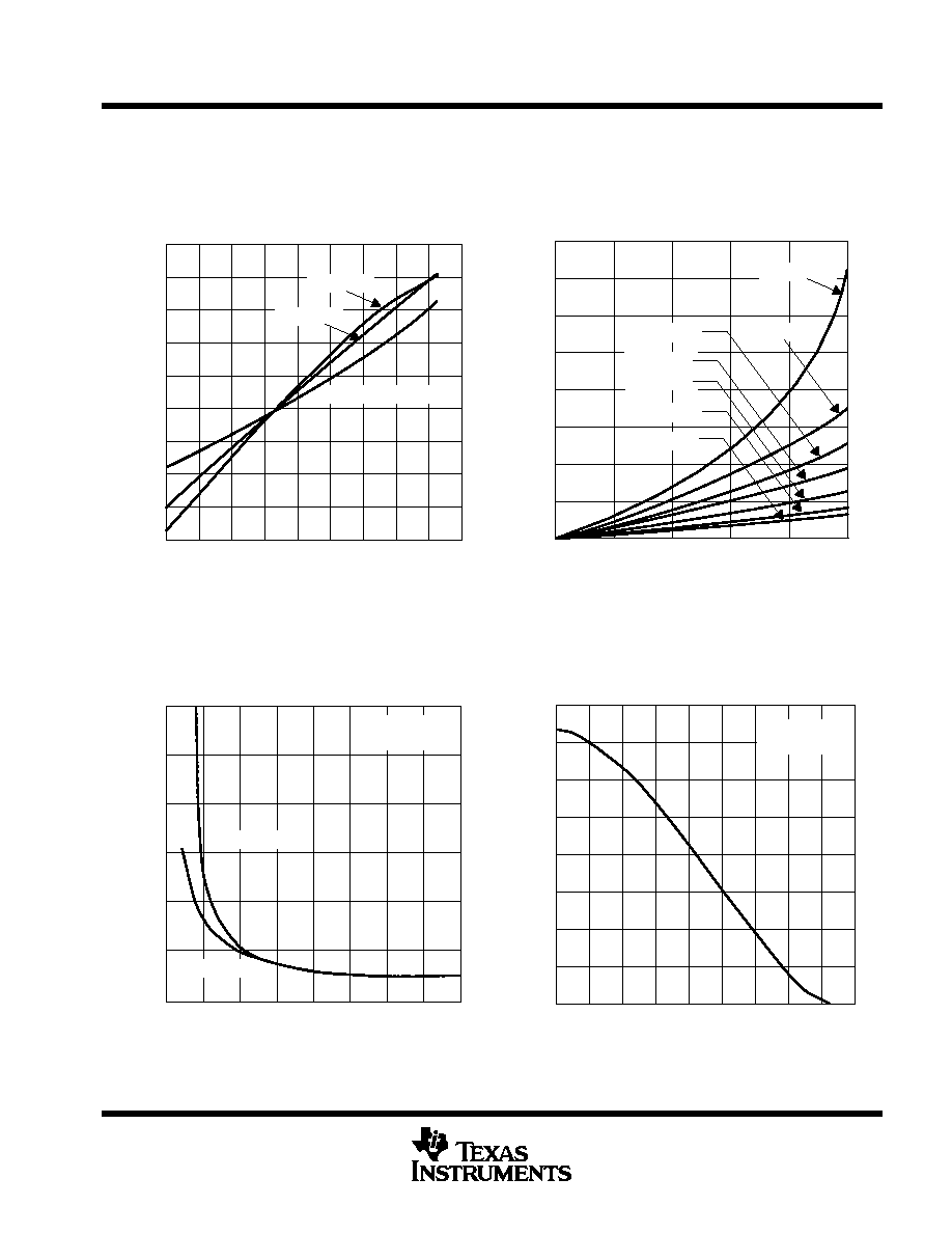
TYPICAL CHARACTERISTICS
Table of Graphs
FIGURE
IQ
Quiescent current
vs Output current
5
IQ
Quiescent current
vs Input voltage
6
IQ
Change in quiescent current
vs Free-air temperature
7
VDO
Dropout voltage
vs Output current
8
VDO
Change in dropout voltage
vs Free-air temperature
9
VDO
Dropout voltage (TPS7201 only)
vs Output current
10
rDS(on)
Pass-element series resistance
vs Input voltage
11
VO
Change in output voltage
vs Free-air temperature
12
VO
Output voltage
vs Input voltage
13
Line regulation
vs Input voltage
14
Load regulation
(TPS7225, TPS7233, TPS7248, TPS7250)
vs Input voltage
15
VO(PG)
Power-good (PG) voltage
vs Output voltage
16
rDS(on)PG
Power-good (PG) on-resistance
vs Input voltage
17
VI
Minimum input voltage for valid PG
vs Free-air temperature
18
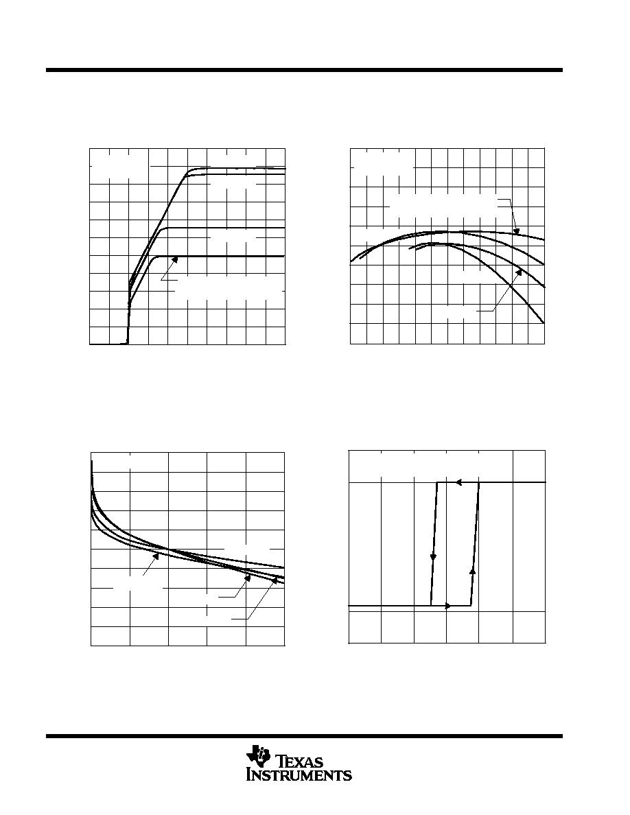
Output voltage response from enable (EN)
vs Time
19
Load transient response (TPS7201/ TPS7233)
vs Time
20
Load transient response (TPS7248/ TPS7250)
vs Time
21
Line transient response (TPS7201)
vs Time
22
Line transient response (TPS7233)
vs Time
23
Line transient response (TPS7248/ TPS7250)
vs Time
24
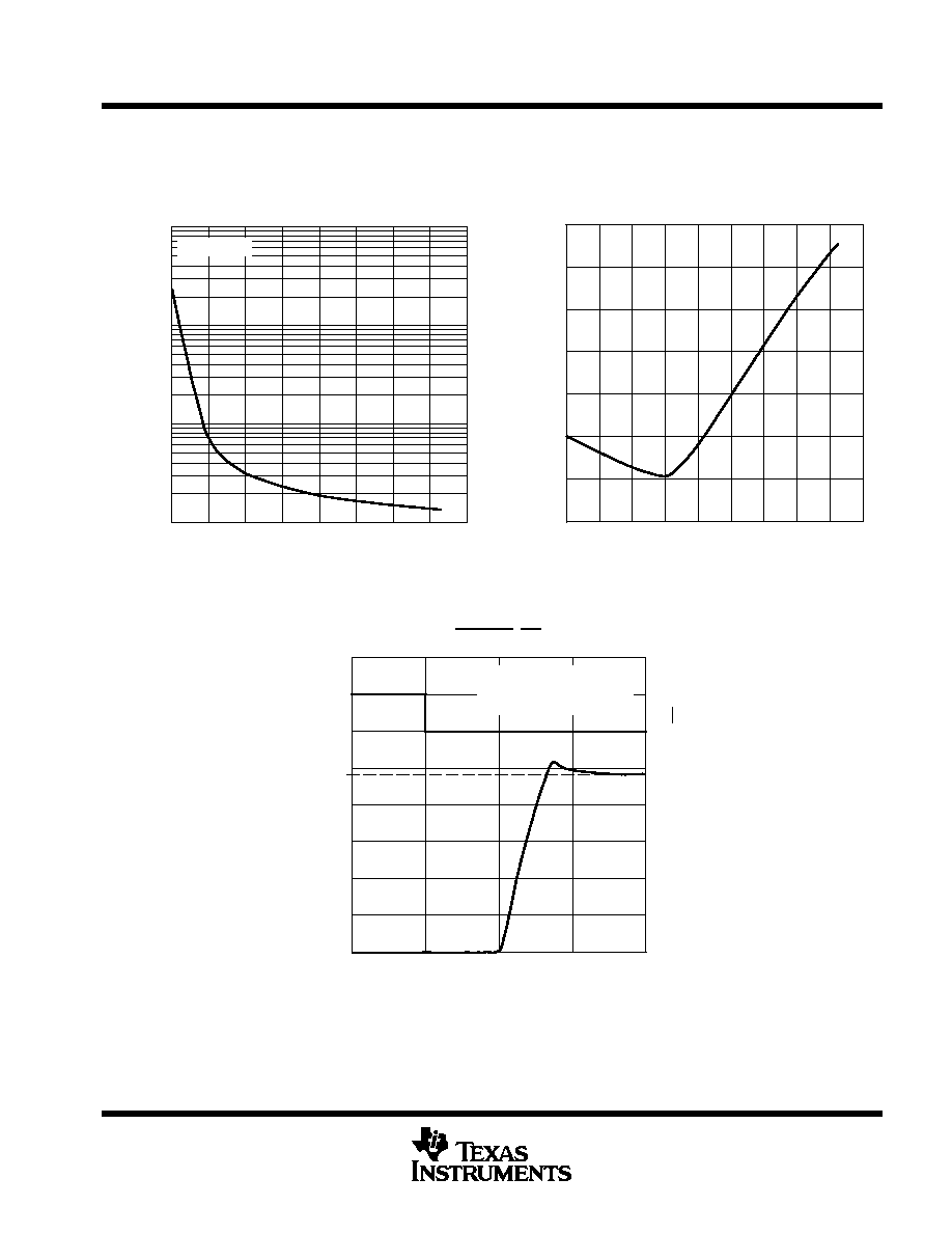
Ripple rejection
vs Frequency
25
Output Spectral Noise Density
vs Frequency
26
vs Output current (CO = 4.7
µ
F)
27
Compensation series resistance (CSR)
vs Added ceramic capacitance (CO = 4.7
µ
F)
28
Compensation series resistance (CSR)
vs Output current (CO = 10
µ
F)
29
vs Added ceramic capacitance (CO = 10
µ
F)
30
This symbol is not currently listed within EIA or JEDEC standards for semiconductor symbology.
TPS7201Q, TPS7225Q, TPS7228Q, TPS7230Q
TPS7233Q, TPS7248Q, TPS7250Q, TPS72xxY
MICROPOWER LOW-DROPOUT (LDO) VOLTAGE REGULATORS
SLVS102F ≠ MARCH 1995 ≠ REVISED NOVEMBER 1998
20
POST OFFICE BOX 655303
∑
DALLAS, TEXAS 75265
TYPICAL CHARACTERISTICS
Figure 5
190
180
160
150
0
50
100
150
≠ Quiescent Current ≠
200
220
QUIESCENT CURRENT
vs
OUTPUT CURRENT
230
200
250
170
210
I Q
A
µ
IO ≠ Output Current ≠ mA
TA = 25
∞
C
TPS7248 VI = 10 V
TPS7233 VI = 10 V
TPS7250 VI = 10 V
TPS7248 VI = 5.85 V
TPS7250 VI = 6.0 V
TPS7233 VI = 4.3 V
Figure 6
100
50
0
0
1
2
3
4
5
6
150
200
QUIESCENT CURRENT
vs
INPUT VOLTAGE
250
7
8
9
10
≠ Quiescent Current ≠
I Q
A
µ
VI ≠ Input Voltage ≠ V
TA 25
∞
C
IO = 250 mA
TPS7248
TPS7233
TPS7250
TPS7201 With
VO Programmed to 2.5 V
Figure 7
10
0
≠ Change in Quiescent Current ≠
30
20
40
CHANGE IN QUIESCENT CURRENT
vs
FREE-AIR TEMPERATURE
50
I Q
A
µ
≠ 10
≠ 20
≠ 30
≠ 40
≠ 40 ≠ 20
0
20
40
60
80
100
120 140
TA ≠ Free-Air Temperature ≠
∞
C
IO = 10 mA
VI = VO + 1 V
Figure 8
200
0
0
50
100
150
≠ Dropout V
oltage ≠ mV
DROPOUT VOLTAGE
vs
OUTPUT CURRENT
400
200
250
100
300
V
DO
IO ≠ Output Current ≠ mA
TPS7233
TPS7248
TPS7250
TA = 25
∞
C
TPS7230
TPS7225
500
600
TPS7201Q, TPS7225Q, TPS7228Q, TPS7230Q
TPS7233Q, TPS7248Q, TPS7250Q, TPS72xxY
MICROPOWER LOW-DROPOUT (LDO) VOLTAGE REGULATORS
SLVS102F ≠ MARCH 1995 ≠ REVISED NOVEMBER 1998
21
POST OFFICE BOX 655303
∑
DALLAS, TEXAS 75265
TYPICAL CHARACTERISTICS
Figure 9
0.01
0
0.03
0.02
0.04
CHANGE IN DROPOUT VOLTAGE
vs
FREE-AIR TEMPERATURE
0.05
≠ Change in Dropout V
oltage ≠ V
V
DO
TA ≠ Free-Air Temperature ≠
∞
C
≠ 0.01
≠ 0.02
≠ 0.03
≠ 0.04
≠ 40 ≠ 20
0
20
40
60
80
100 120
140
TPS7233
TPS7248/TPS7250
TPS7230
Figure 10
0
50
100
150
200
250
1.6
1.4
1.2
1
0.8
0.6
0.4
0.2
0
≠ Dropout V
oltage ≠ V
V
DO
IO ≠ Output Current ≠ mA
TPS7201
DROPOUT VOLTAGE
vs
OUTPUT CURRENT
VI = 2.9 V
VI = 2.4 V
VI = 2.6 V
VI = 3.2 V
VI = 3.9 V
VI = 5.9 V
VI = 9.65 V
This voltage is not recommended.
Figure 11
3
2
1
0
2
3
4
5
6
7
≠ Pass Element Series Resistance ≠
4
5
PASS ELEMENT SERIES RESISTANCE
vs
INPUT VOLTAGE
6
8
9
10
r
DS(on)
VI ≠ Input Voltage ≠ V
TA = 25
∞
C
VFB = 1.12 V
IO = 250 mA
IO = 100 mA
Figure 12
CHANGE IN OUTPUT VOLTAGE
vs
FREE-AIR TEMPERATURE
≠ Change in Output V
oltage ≠ mV
V
O
TA ≠ Free-Air Temperature ≠
∞
C
15
10
5
0
≠ 5
≠ 10
≠ 15
≠ 20
≠ 25
≠ 40
≠ 20
0
20
40
60
80
100
120
140
IO = 10 mA
VI = VO + 1 V
TPS7201Q, TPS7225Q, TPS7228Q, TPS7230Q
TPS7233Q, TPS7248Q, TPS7250Q, TPS72xxY
MICROPOWER LOW-DROPOUT (LDO) VOLTAGE REGULATORS
SLVS102F ≠ MARCH 1995 ≠ REVISED NOVEMBER 1998
22
POST OFFICE BOX 655303
∑
DALLAS, TEXAS 75265
TYPICAL CHARACTERISTICS
Figure 13
3
2
1
0
0
1
2
3
4
5
6
≠ Output V
oltage ≠ V
4
4.5
OUTPUT VOLTAGE
vs
INPUT VOLTAGE
5.5
7
8
9
10
5
3.5
2.5
1.5
0.5
V
O
VI ≠ Input Voltage ≠ V
TPS7250
TPS7248
TPS7233
TA = 25
∞
C
IO = 250 mA
TPS7201 With
VO Programmed to 2.5 V
Figure 14
4
4.5
5
6 6.5
7 7.5
LINE REGULATION
8
8.5
9.5 10
5.5
9
25
20
15
10
5
0
≠ 5
≠ 10
≠ 15
≠ 20
≠ 25
TPS7250
TPS7233
TPS7248
TA = 25
∞
C
IO = 250 mA
≠ Change in Output V
oltage ≠ mV
V
O
VI ≠ Input Voltage ≠ V
TPS7201 With
VO Programmed to 2.5 V
Figure 15
0
50
100
150
200
250
50
40
30
20
10
0
≠ 10
≠ 20
≠ 30
≠ 40
≠ 50
IO ≠ Output Current ≠ mA
TA = 25
∞
C
≠ Change in Output V
oltage ≠ mV
V
O
TPS7233
TPS7250
TPS7248
TPS7225
LOAD REGULATION
Figure 16
POWER-GOOD (PG) VOLTAGE
vs
OUTPUT VOLTAGE
GND
0
92
93
94
95
≠ Power-Good (PG) V
oltage ≠ V
6
96
98
TA = 25
∞
C
PG Pulled Up to VI With 5 k
Resistor
VO ≠ Output Voltage ≠ %
¡¡
¡¡
V
O(PG)
97
VI
VO as a percent of VOnom.
TPS7201Q, TPS7225Q, TPS7228Q, TPS7230Q
TPS7233Q, TPS7248Q, TPS7250Q, TPS72xxY
MICROPOWER LOW-DROPOUT (LDO) VOLTAGE REGULATORS
SLVS102F ≠ MARCH 1995 ≠ REVISED NOVEMBER 1998
23
POST OFFICE BOX 655303
∑
DALLAS, TEXAS 75265
TYPICAL CHARACTERISTICS
Figure 17
10
1
0
100
1
1.5
2
2.5
3
3.5
4
≠ Power-Good (PG) On-Resistance ≠ k
POWER-GOOD (PG) ON-RESISTANCE
vs
INPUT VOLTAGE
4.5
5
r DS(on)
VI ≠ Input Voltage ≠ V
TA = 25
∞
C
Figure 18
1.125
1.095
≠ Minimum Input V
oltage for V
alid PG
1.115
1.11
1.12
MINIMUM INPUT VOLTAGE FOR VALID PG
vs
FREE-AIR TEMPERATURE
1.3
≠ 40 ≠ 20
0
20
40
60
80
100 120 140
¡¡
V
I
1.105
TA ≠ Free-Air Temperature ≠
∞
C
1.1
≠ Output V
oltage ≠ V
OUTPUT VOLTAGE RESPONSE FROM
ENABLE (EN)
0
50
100
150
5
0
≠ EN V
oltage ≠ V
V
O
VO nom
V
I(EN)
t ≠ Time ≠
µ
s
(V
alues V
ary
W
ith
Selection of Device)
10
TA = 25
∞
C
CI = 0
CO = 4.7
µ
F (CSR = 1
)
Figure 19
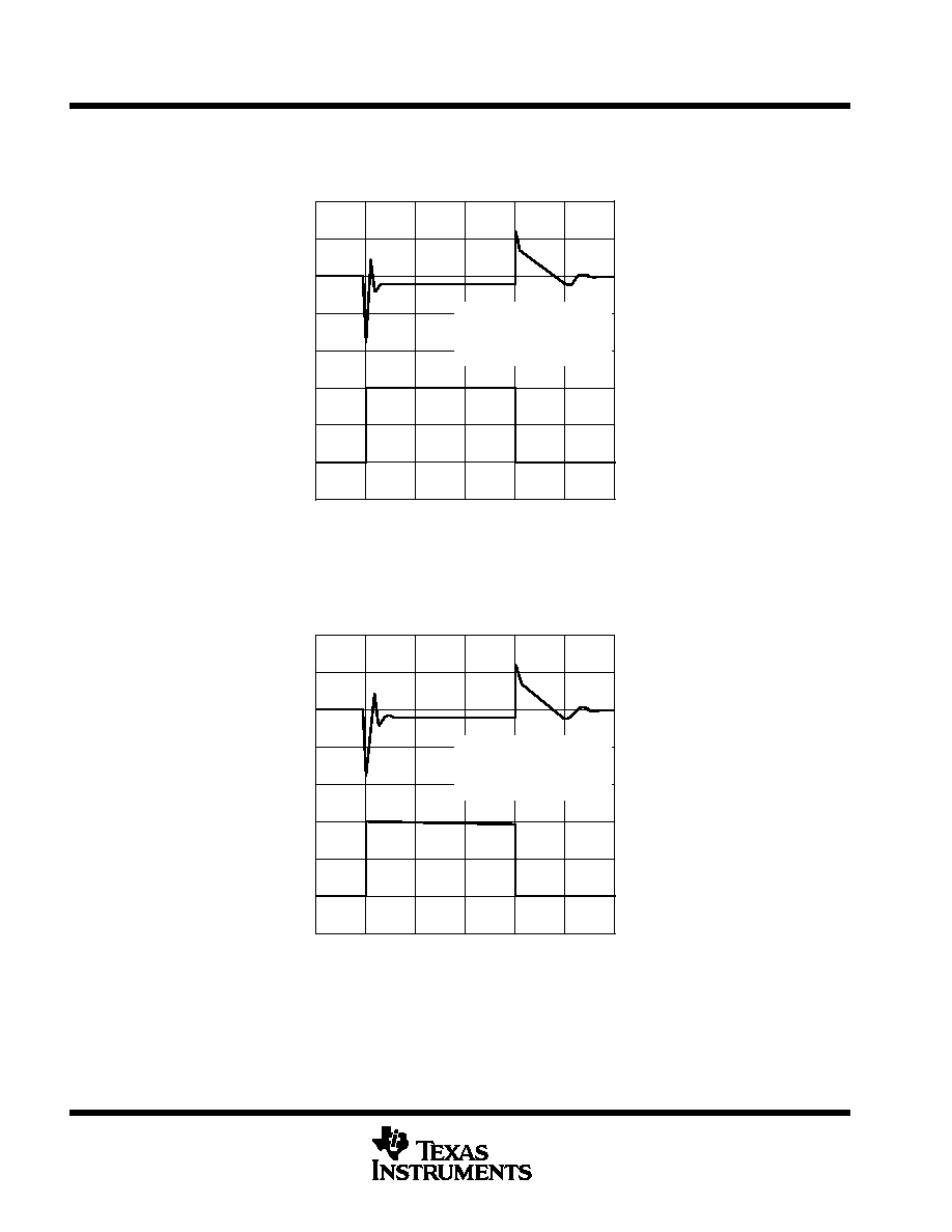
TPS7201Q, TPS7225Q, TPS7228Q, TPS7230Q
TPS7233Q, TPS7248Q, TPS7250Q, TPS72xxY
MICROPOWER LOW-DROPOUT (LDO) VOLTAGE REGULATORS
SLVS102F ≠ MARCH 1995 ≠ REVISED NOVEMBER 1998
24
POST OFFICE BOX 655303
∑
DALLAS, TEXAS 75265
TYPICAL CHARACTERISTICS
TPS7201 (WITH VO PROGRAMMED TO 2.5 V)
,
TPS7233
LOAD TRANSIENT RESPONSE
200
100
0
≠ 100
≠ 200
≠ Output Current ≠ mA
105
55
5
I O
t ≠ Time ≠
µ
s
0
100
200
300
400
500
TA = 25
∞
C
VI = 6 V
CI = 0
CO = 4.7
µ
F (CSR = 1
)
≠ Change in Output V
oltage ≠ mV
V
O
Figure 20
LOAD TRANSIENT RESPONSE
200
100
0
≠ 100
≠ 200
105
55
5
TPS7248/TPS7250
t ≠ Time ≠
µ
s
0
100
200
300
400
500
TA = 25
∞
C
VI = 6 V
CI = 0
CO = 4.7
µ
F (CSR = 1
)
≠ Change in Output V
oltage ≠ mV
V
O
≠ Output Current ≠ mA
I O
Figure 21
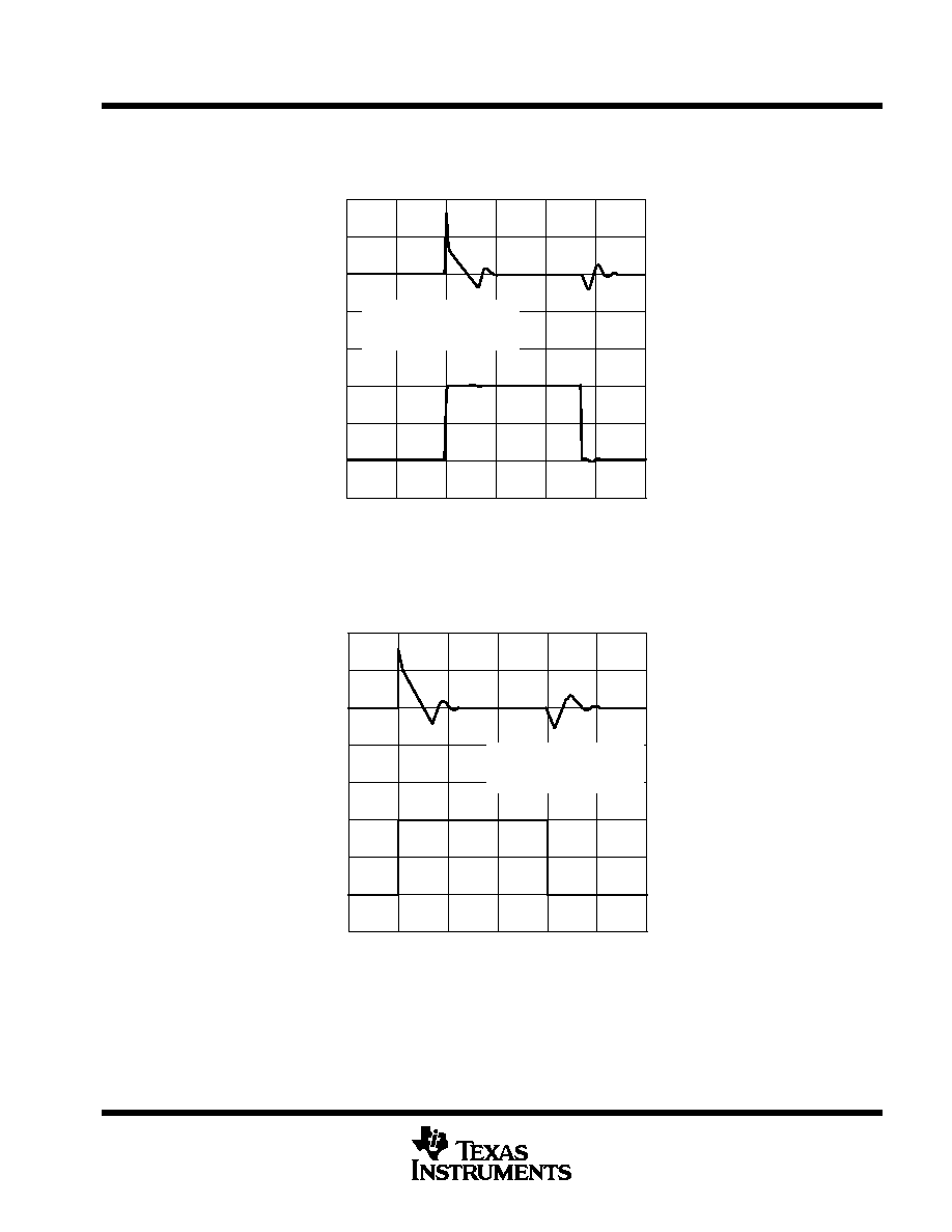
TPS7201Q, TPS7225Q, TPS7228Q, TPS7230Q
TPS7233Q, TPS7248Q, TPS7250Q, TPS72xxY
MICROPOWER LOW-DROPOUT (LDO) VOLTAGE REGULATORS
SLVS102F ≠ MARCH 1995 ≠ REVISED NOVEMBER 1998
25
POST OFFICE BOX 655303
∑
DALLAS, TEXAS 75265
TYPICAL CHARACTERISTICS
LINE TRANSIENT RESPONSE
100
50
0
≠ 50
≠ 100
6.5
6.25
6
TPS7201 WITH VO PROGRAMMED TO 2.5 V
t ≠ Time ≠
µ
s
0
100
200
300
400
TA = 25
∞
C
CI = 0
CO = 4.7
µ
F (CSR = 1
)
≠ Change in Output V
oltage ≠ mV
V
O
≠ Input V
oltage ≠ V
V
I
Figure 22
LINE TRANSIENT RESPONSE
200
100
0
≠ 50
≠ 100
≠ Input V
oltage ≠ V
6.5
6.25
6
V
I
TPS7233
t ≠ Time ≠
µ
s
5.75
0
100
200
300
400
500
TA = 25
∞
C
CI = 0
CO = 4.7
µ
F (CSR = 1
)
≠ Change in Output V
oltage ≠ mV
V
O
Figure 23
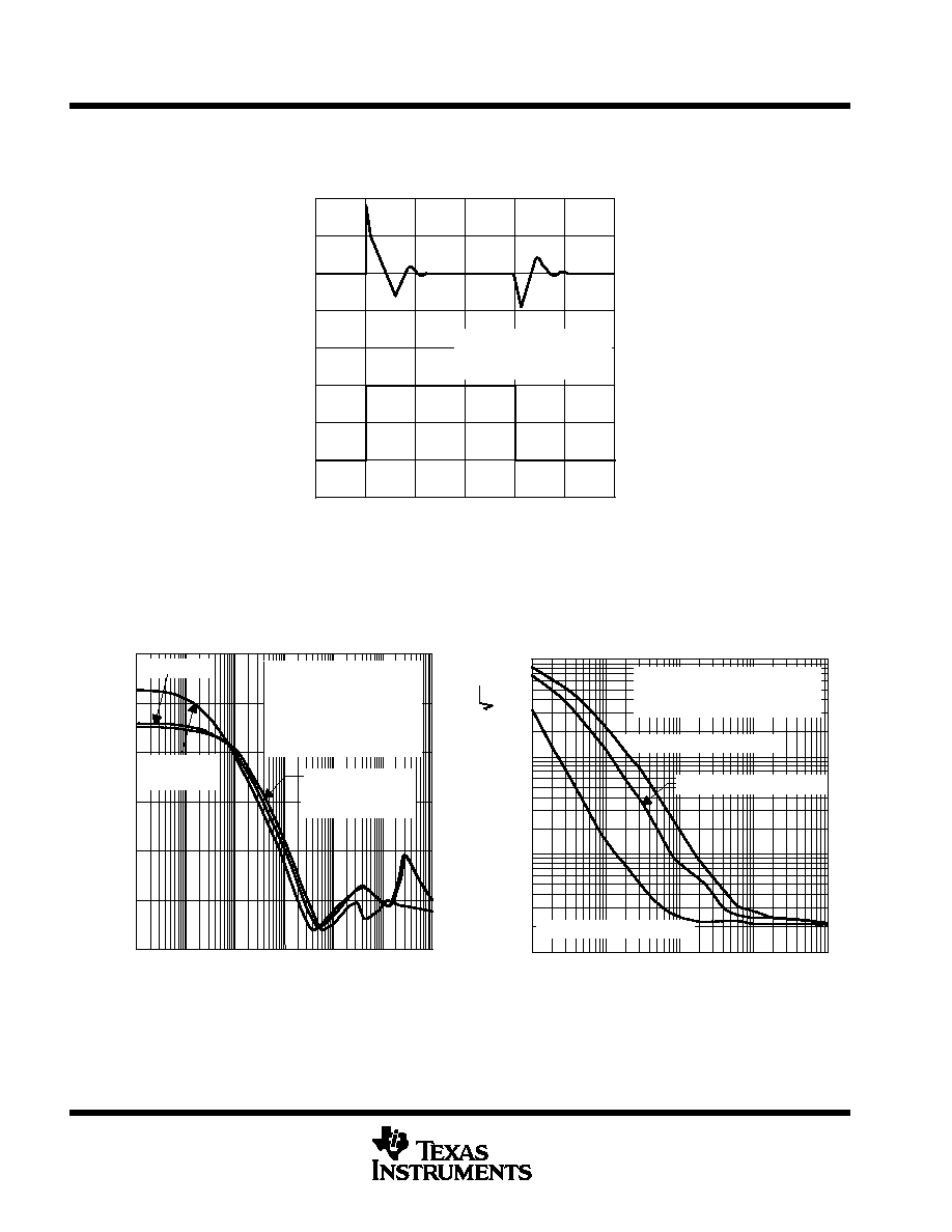
TPS7201Q, TPS7225Q, TPS7228Q, TPS7230Q
TPS7233Q, TPS7248Q, TPS7250Q, TPS72xxY
MICROPOWER LOW-DROPOUT (LDO) VOLTAGE REGULATORS
SLVS102F ≠ MARCH 1995 ≠ REVISED NOVEMBER 1998
26
POST OFFICE BOX 655303
∑
DALLAS, TEXAS 75265
TYPICAL CHARACTERISTICS
LINE TRANSIENT RESPONSE
100
50
0
≠ 50
≠ 100
≠ Input V
oltage ≠ V
6.5
6.25
6
V
I
TPS7248/TPS7250
t ≠ Time ≠
µ
s
0
100
200
300
400
500
TA = 25
∞
C
CI = 0
CO = 4.7
µ
F (CSR = 1
)
≠ Change in Output V
oltage ≠ mV
V
O
Figure 24
Figure 25
30
10
0
Ripple Rejection ≠ dB
40
50
f ≠ Frequency ≠ Hz
RIPPLE REJECTION
vs
FREQUENCY
60
20
10
100
1 K
10 K
100 K
1 M
10 M
TA = 25
∞
C
No Input
Capacitance Added
VI = VO + 1 V
IO = 100 mA
CO = 4.7
µ
F (CSR = 1
)
TPS7233
TPS7201 With
VO Programmed
to 2.5 V
TPS7248/
TPS7250
Figure 26
10
100
1 k
10 k
100 k
CO = 10
µ
F (CSR = 1
)
CO = 4.7
µ
F (CSR = 1
)
CO = 100
µ
F (CSR = 1
)
f ≠ Frequency ≠ Hz
OUTPUT SPECTRAL NOISE DENSITY
vs
FREQUENCY
10
1
0.1
0.01
TA = 25
∞
C
No Input Capacitance Added
VI = VO + 1 V
Output Spectral Noise Density ≠
V/
Hz
µ
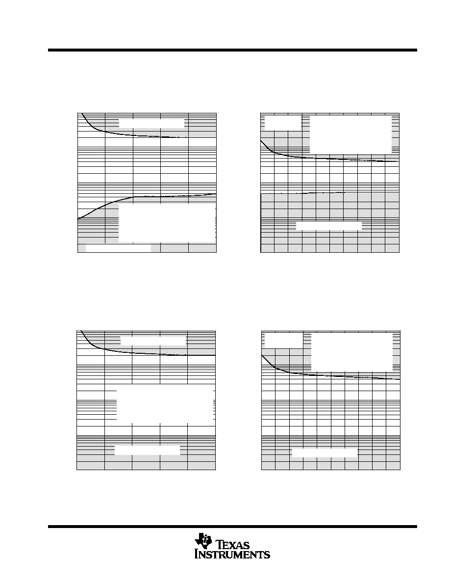
TPS7201Q, TPS7225Q, TPS7228Q, TPS7230Q
TPS7233Q, TPS7248Q, TPS7250Q, TPS72xxY
MICROPOWER LOW-DROPOUT (LDO) VOLTAGE REGULATORS
SLVS102F ≠ MARCH 1995 ≠ REVISED NOVEMBER 1998
27
POST OFFICE BOX 655303
∑
DALLAS, TEXAS 75265
TYPICAL CHARACTERISTICS
Figure 27
0.1
0.01
0
50
100
150
200
250
TYPICAL REGIONS OF STABILITY
COMPENSATION SERIES RESISTANCE (CSR)
vs
OUTPUT CURRENT
10
100
IO ≠ Output Current ≠ mA
CSR ≠ Compensation Series Resistance ≠
Region of Instability
1
TA = 25
∞
C
VI = VO + 1 V
CO = 4.7
µ
F
No Added Ceramic Capacitance
No Input Capacitance Added
Region of Instability
Figure 28
0.1
0.01
0
0.1
0.2
0.3
0.4
0.5
TYPICAL REGIONS OF STABILITY
COMPENSATION SERIES RESISTANCE (CSR)
vs
ADDED CERAMIC CAPACITANCE
10
100
Added Ceramic Capacitance ≠
µ
F
0.6
0.7 0.8
0.9
1
1
TA = 25
∞
C
VI = VO + 1 V
IO = 250 mA
CO = 4.7
µ
F
No Input Capacitor Added
Region of Instability
Region of
Instability
CSR ≠ Compensation Series Resistance ≠
Figure 29
0.1
0.01
0
50
100
150
200
250
TYPICAL REGIONS OF STABILITY
COMPENSATION SERIES RESISTANCE (CSR)
vs
OUTPUT CURRENT
10
100
IO ≠ Output Current ≠ mA
1
Region of Instability
TA = 25
∞
C
VI = VO + 1 V
CO = 10
µ
F
No Added Ceramic Capacitance
No Input Capacitor Added
Region of Instability
CSR ≠ Compensation Series Resistance ≠
Figure 30
0.1
0.01
0
0.1
0.2
0.3
0.4
0.5
TYPICAL REGIONS OF STABILITY
COMPENSATION SERIES RESISTANCE (CSR)
vs
ADDED CERAMIC CAPACITANCE
10
100
Added Ceramic Capacitance ≠
µ
F
1
0.6
0.7 0.8
0.9
1
Region of Instability
TA = 25
∞
C
VI = VO + 1 V
IO = 250 mA
CO = 10
µ
F
No Input Capacitor Added
Region of
Instability
CSR ≠ Compensation Series Resistance ≠
CSR refers to the total series resistance, including the ESR of the capacitor, any series resistance added externally, and PWB trace resistance
to CO.

TPS7201Q, TPS7225Q, TPS7228Q, TPS7230Q
TPS7233Q, TPS7248Q, TPS7250Q, TPS72xxY
MICROPOWER LOW-DROPOUT (LDO) VOLTAGE REGULATORS
SLVS102F ≠ MARCH 1995 ≠ REVISED NOVEMBER 1998
28
POST OFFICE BOX 655303
∑
DALLAS, TEXAS 75265
APPLICATION INFORMATION
The design of the TPS72xx family of low-dropout (LDO) regulators is based on the higher-current TPS71xx
family. These new families of regulators have been optimized for use in battery-operated equipment and feature
extremely low dropout voltages, low supply currents that remain constant over the full-output-current range of
the device, and an enable input to reduce supply currents to less than 0.5
µ
A when the regulator is turned off.
device operation
The TPS72xx uses a PMOS pass element to dramatically reduce both dropout voltage and supply current over
more conventional PNP-pass-element LDO designs. The PMOS transistor is a voltage-controlled device that,
unlike a PNP transistor, does not require increased drive current as output current increases. Supply current
in the TPS72xx is essentially constant from no-load to maximum.
Current limiting and thermal protection prevent damage by excessive output current and/or power dissipation.
The device switches into a constant-current mode at approximately 1 A; further load increases reduce the output
voltage instead of increasing the output current. The thermal protection shuts the regulator off if the junction
temperature rises above 165
∞
C. Recovery is automatic when the junction temperature drops approximately 5
∞
C
below the high temperature trip point. The PMOS pass element includes a back diode that safely conducts
reverse current when the input voltage level drops below the output voltage level.
A logic high on the enable input, EN, shuts off the output and reduces the supply current to less than 0.5
µ
A.
EN should be grounded in applications where the shutdown feature is not used.
Power good (PG) is an open-drain output signal used to indicate output-voltage status. A comparator circuit
continuously monitors the output voltage. When the output drops to approximately 95% of its nominal regulated
value, the comparator turns on and pulls PG low.
Transient loads or line pulses can also cause activation of PG if proper care is not taken in selecting the input
and output capacitors. Load transients that are faster than 5
µ
s can cause a signal on PG if high-ESR output
capacitors (greater than approximately 7
) are used. A 1-
µ
s transient causes a PG signal when using an output
capacitor with greater than 3.5
of ESR. It is interesting to note that the output-voltage spike during the transient
can drop well below the reset threshold and still not trip if the transient duration is short. A 1-
µ
s transient must
drop at least 500 mV below the threshold before tripping the PG circuit. A 2-
µ
s transient trips PG at just 400 mV
below the threshold. Lower-ESR output capacitors help by reducing the drop in output voltage during a transient
and should be used when fast transients are expected.
A typical application circuit is shown in Figure 31.
TPS7201Q, TPS7225Q, TPS7228Q, TPS7230Q
TPS7233Q, TPS7248Q, TPS7250Q, TPS72xxY
MICROPOWER LOW-DROPOUT (LDO) VOLTAGE REGULATORS
SLVS102F ≠ MARCH 1995 ≠ REVISED NOVEMBER 1998
29
POST OFFICE BOX 655303
∑
DALLAS, TEXAS 75265
APPLICATION INFORMATION
C1
0.1
µ
F
NOTE A: TPS7225, TPS7228, TPS7230, TPS7233, TPS7248,
TPS7250 (fixed-voltage options).
SENSE
PG
OUT
OUT
6
5
4
IN
IN
EN
GND
3
2
1
7
8
VI
PG
CSR = 1
VO
10
µ
F
+
TPS72xx
(see Note A)
250 k
This device is in the product preview stage of development.
Please contact the local TI sales office for availability.
Figure 31. Typical Application Circuit
external capacitor requirements
Although not required, a 0.047-
µ
F to 0.1-
µ
F ceramic bypass input capacitor, connected between IN and GND
and located close to the TPS72xx, is recommended to improve transient response and noise rejection. A
higher-value electrolytic input capacitor may be necessary if large, fast-rise-time load transients are anticipated
and the device is located several inches from the power source.
An output capacitor is required to stabilize the internal feedback loop. For most applications, a 10-
µ
F to 15-
µ
F
solid-tantalum capacitor with a 0.5-
resistor (see capacitor selection table) in series is sufficient. The maximum
capacitor ESR should be limited to 1.3
to allow for ESR doubling at cold temperatures. Figure 32 shows the
transient response of a 5-mA to 85-mA load using a 10-
µ
F output capacitor with a total ESR of 1.7
.
A 4.7-
µ
F solid-tantalum capacitor in series with a 1-
resistor may also be used (see Figures 27 and 28)
provided the ESR of the capacitor does not exceed 1
at room temperature and 2
over the full operating
temperature range.
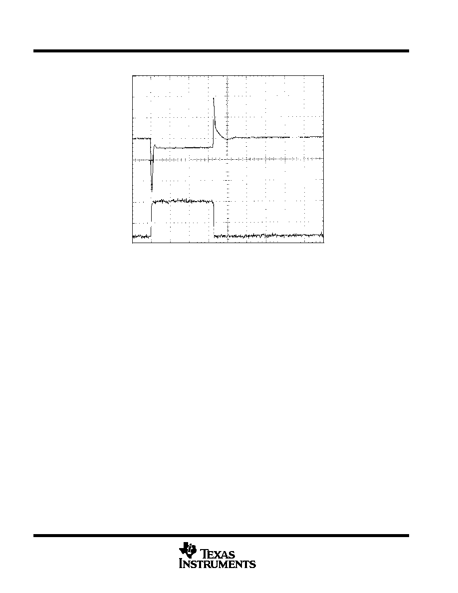
TPS7201Q, TPS7225Q, TPS7228Q, TPS7230Q
TPS7233Q, TPS7248Q, TPS7250Q, TPS72xxY
MICROPOWER LOW-DROPOUT (LDO) VOLTAGE REGULATORS
SLVS102F ≠ MARCH 1995 ≠ REVISED NOVEMBER 1998
30
POST OFFICE BOX 655303
∑
DALLAS, TEXAS 75265
APPLICATION INFORMATION
2
1
Ch 2
VO
IO = 5 mA
Ch1
50 mV
50 mA
100
µ
s/div
VI = VO + 1 V
IO = 85 mA
Figure 32. Load Transient Response (CSR total = 1.7
), TPS7248Q
A partial listing of surface-mount capacitors usable with the TPS72xx family is provided below. This information
(along with the stability graphs, Figures 27 through 30) is included to assist the designer in selecting suitable
capacitors.
CAPACITOR SELECTION
PART NO.
MFR.
VALUE
MAX ESR
SIZE (H
◊
L
◊
W)
592D156X0020R2T
Sprague
15
µ
F, 20 V
1.1
1.2
◊
7.2
◊
6
595D156X0025C2T
Sprague
15
µ
F, 25 V
1
2.5
◊
7.1
◊
3.2
595D106X0025C2T
Sprague
10
µ
F, 25 V
1.2
2.5
◊
7.1
◊
3.2
695D106X0035G2T
Sprague
10
µ
F, 35 V
1.3
2.5
◊
7.6
◊
2.5
Size is in mm. ESR is maximum resistance in ohms at 100 kHz and TA = 25
∞
C. Listings are sorted by height.
sense-pin connection
SENSE must be connected to OUT for proper operation of the regulator. Normally this connection should be
as short as possible; however, remote sense may be implemented in critical applications when proper care of
the circuit path is exercised. SENSE internally connects to a high-impedance wide-bandwidth amplifier through
a resistor-divider network, and any noise pickup on the PCB trace will feed through to the regulator output.
SENSE must be routed to minimize noise pickup. Filtering SENSE using an RC network is not recommended
because of the possibility of inducing regulator instability.
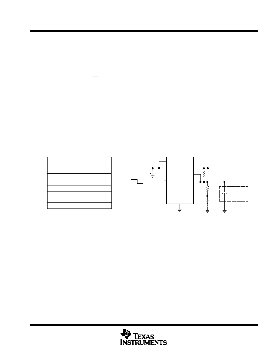
TPS7201Q, TPS7225Q, TPS7228Q, TPS7230Q
TPS7233Q, TPS7248Q, TPS7250Q, TPS72xxY
MICROPOWER LOW-DROPOUT (LDO) VOLTAGE REGULATORS
SLVS102F ≠ MARCH 1995 ≠ REVISED NOVEMBER 1998
31
POST OFFICE BOX 655303
∑
DALLAS, TEXAS 75265
APPLICATION INFORMATION
output voltage programming
The output voltage of the TPS7201 adjustable regulator is programmed using an external resistor divider as
shown in Figure 33. The output voltage is calculated using:
V
O
+
V
ref
@
1
)
R1
R2
(1)
Where
V
ref
= 1.188 V typ (the internal reference voltage)
Resistors R1 and R2 should be chosen for approximately 7-
µ
A divider current. Lower value resistors can be
used but offer no inherent advantage and waste more power. Higher values should be avoided as leakage
currents at FB increase the output voltage error. The recommended design procedure is to choose
R2 = 169 k
to set the divider current at 7
µ
A and then calculate R1 using:
R1
+
V
O
V
ref
*
1
@
R2
(2)
VO
VI
PG
OUT
FB
R2
GND
EN
IN
<0.4 V
>2.7 V
TPS7201
Power-Good Indicator
0.1
µ
F
250 k
OUTPUT
VOLTAGE
(V)
R1
R2
2.5
3.3
3.6
4
5
6.4
191
309
348
402
549
750
169
169
169
169
169
169
OUTPUT VOLTAGE
PROGRAMMING GUIDE
DIVIDER RESISTANCE
(k
)
1% values shown.
10
µ
F
CSR = 1
IN
5
6
4
2
8
7
1
3
+
OUT
R1
Figure 33. TPS7201 Adjustable LDO Regulator Programming
TPS7201Q, TPS7225Q, TPS7228Q, TPS7230Q
TPS7233Q, TPS7248Q, TPS7250Q, TPS72xxY
MICROPOWER LOW-DROPOUT (LDO) VOLTAGE REGULATORS
SLVS102F ≠ MARCH 1995 ≠ REVISED NOVEMBER 1998
32
POST OFFICE BOX 655303
∑
DALLAS, TEXAS 75265
APPLICATION INFORMATION
power dissipation and junction temperature
Specified regulator operation is assured to a junction temperature of 125
∞
C; the maximum junction temperature
allowable to avoid damaging the device is 150
∞
C. These restrictions limit the power dissipation that the regulator
can handle in any given application. To ensure the junction temperature is within acceptable limits, calculate
the maximum allowable dissipation, P
D(max)
, and the actual dissipation, P
D
, which must be less than or equal
to P
D(max)
.
The maximum-power-dissipation limit is determined using the following equation:
P
D(max)
+
T
J
max
*
T
A
R
q
JA
Where
T
J
max
is the maximum allowable junction temperature, i.e.,150
∞
C absolute maximum and 125
∞
C
recommended operating temperature.
R
JA
is the thermal resistance junction-to-ambient for the package, i.e., 172
∞
C/W for the 8-terminal
SOIC and 238
∞
C/W for the 8-terminal TSSOP.
T
A
is the ambient temperature.
The regulator dissipation is calculated using:
P
D
+
V
I
*
V
O
@
I
O
Power dissipation resulting from quiescent current is negligible.
regulator protection
The TPS72xx PMOS-pass transistor has a built-in back diode that safely conducts reverse currents when the
input voltage drops below the output voltage (e.g., during power down). Current is conducted from the output
to the input and is not internally limited. If extended reverse voltage is anticipated, external limiting might be
appropriate.
The TPS72xx also features internal current limiting and thermal protection. During normal operation, the
TPS72xx limits output current to approximately 1 A. When current limiting engages, the output voltage scales
back linearly until the overcurrent condition ends. While current limiting is designed to prevent gross device
failure, care should be taken not to exceed the power dissipation ratings of the package. If the temperature of
the device exceeds 165
∞
C, thermal-protection circuitry shuts it down. Once the device has cooled, regulator
operation resumes.
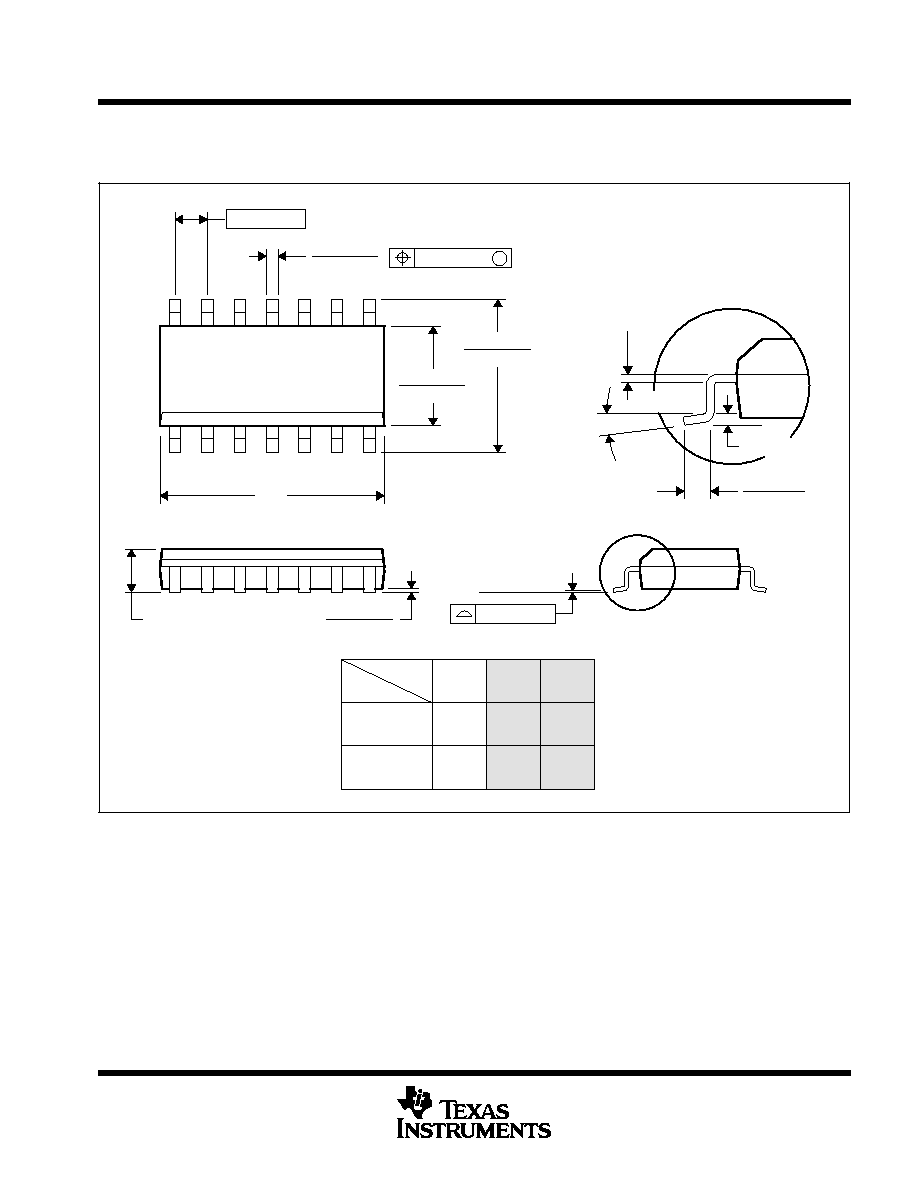
TPS7201Q, TPS7225Q, TPS7228Q, TPS7230Q
TPS7233Q, TPS7248Q, TPS7250Q, TPS72xxY
MICROPOWER LOW-DROPOUT (LDO) VOLTAGE REGULATORS
SLVS102F ≠ MARCH 1995 ≠ REVISED NOVEMBER 1998
33
POST OFFICE BOX 655303
∑
DALLAS, TEXAS 75265
MECHANICAL DATA
D (R-PDSO-G**)
PLASTIC SMALL-OUTLINE PACKAGE
14 PIN SHOWN
4040047 / D 10/96
0.228 (5,80)
0.244 (6,20)
0.069 (1,75) MAX
0.010 (0,25)
0.004 (0,10)
1
14
0.014 (0,35)
0.020 (0,51)
A
0.157 (4,00)
0.150 (3,81)
7
8
0.044 (1,12)
0.016 (0,40)
Seating Plane
0.010 (0,25)
PINS **
0.008 (0,20) NOM
A MIN
A MAX
DIM
Gage Plane
0.189
(4,80)
(5,00)
0.197
8
(8,55)
(8,75)
0.337
14
0.344
(9,80)
16
0.394
(10,00)
0.386
0.004 (0,10)
M
0.010 (0,25)
0.050 (1,27)
0
∞
≠ 8
∞
NOTES: B. All linear dimensions are in inches (millimeters).
C. This drawing is subject to change without notice.
D. Body dimensions do not include mold flash or protrusion, not to exceed 0.006 (0,15).
E. Falls within JEDEC MS-012
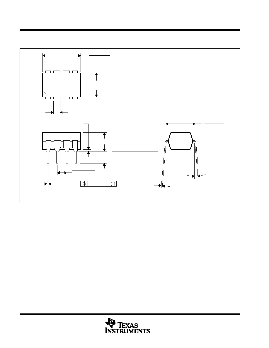
TPS7201Q, TPS7225Q, TPS7228Q, TPS7230Q
TPS7233Q, TPS7248Q, TPS7250Q, TPS72xxY
MICROPOWER LOW-DROPOUT (LDO) VOLTAGE REGULATORS
SLVS102F ≠ MARCH 1995 ≠ REVISED NOVEMBER 1998
34
POST OFFICE BOX 655303
∑
DALLAS, TEXAS 75265
MECHANICAL DATA
P (R-PDIP-T8)
PLASTIC DUAL-IN-LINE PACKAGE
4040082 / B 03/95
0.310 (7,87)
0.290 (7,37)
0.010 (0,25) NOM
0.400 (10,60)
0.355 (9,02)
5
8
4
1
0.020 (0,51) MIN
0.070 (1,78) MAX
0.240 (6,10)
0.260 (6,60)
0.200 (5,08) MAX
0.125 (3,18) MIN
0.015 (0,38)
0.021 (0,53)
Seating Plane
M
0.010 (0,25)
0.100 (2,54)
0
∞
≠ 15
∞
NOTES: A. All linear dimensions are in inches (millimeters).
B. This drawing is subject to change without notice.
C. Falls within JEDEC MS-001
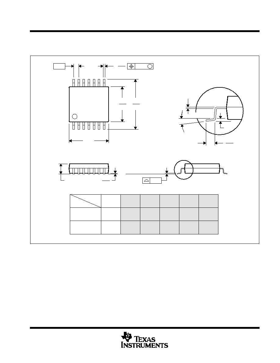
TPS7201Q, TPS7225Q, TPS7228Q, TPS7230Q
TPS7233Q, TPS7248Q, TPS7250Q, TPS72xxY
MICROPOWER LOW-DROPOUT (LDO) VOLTAGE REGULATORS
SLVS102F ≠ MARCH 1995 ≠ REVISED NOVEMBER 1998
35
POST OFFICE BOX 655303
∑
DALLAS, TEXAS 75265
MECHANICAL DATA
PW (R-PDSO-G**)
PLASTIC SMALL-OUTLINE PACKAGE
4040064 / E 08/96
14 PIN SHOWN
Seating Plane
1,20 MAX
1
A
7
14
0,19
4,50
4,30
8
6,20
6,60
0,30
0,75
0,50
0,25
Gage Plane
0,15 NOM
0,65
M
0,10
0
∞
≠ 8
∞
0,10
PINS **
A MIN
A MAX
DIM
2,90
3,10
8
4,90
5,10
14
6,60
6,40
4,90
5,10
16
7,70
20
7,90
24
9,60
9,80
28
0,15
0,05
NOTES: A. All linear dimensions are in millimeters.
B. This drawing is subject to change without notice.
C. Body dimensions do not include mold flash or protrusion not to exceed 0,15.
D. Falls within JEDEC MO-153

IMPORTANT NOTICE
Texas Instruments and its subsidiaries (TI) reserve the right to make changes to their products or to discontinue
any product or service without notice, and advise customers to obtain the latest version of relevant information
to verify, before placing orders, that information being relied on is current and complete. All products are sold
subject to the terms and conditions of sale supplied at the time of order acknowledgement, including those
pertaining to warranty, patent infringement, and limitation of liability.
TI warrants performance of its semiconductor products to the specifications applicable at the time of sale in
accordance with TI's standard warranty. Testing and other quality control techniques are utilized to the extent
TI deems necessary to support this warranty. Specific testing of all parameters of each device is not necessarily
performed, except those mandated by government requirements.
CERTAIN APPLICATIONS USING SEMICONDUCTOR PRODUCTS MAY INVOLVE POTENTIAL RISKS OF
DEATH, PERSONAL INJURY, OR SEVERE PROPERTY OR ENVIRONMENTAL DAMAGE ("CRITICAL
APPLICATIONS"). TI SEMICONDUCTOR PRODUCTS ARE NOT DESIGNED, AUTHORIZED, OR
WARRANTED TO BE SUITABLE FOR USE IN LIFE-SUPPORT DEVICES OR SYSTEMS OR OTHER
CRITICAL APPLICATIONS. INCLUSION OF TI PRODUCTS IN SUCH APPLICATIONS IS UNDERSTOOD TO
BE FULLY AT THE CUSTOMER'S RISK.
In order to minimize risks associated with the customer's applications, adequate design and operating
safeguards must be provided by the customer to minimize inherent or procedural hazards.
TI assumes no liability for applications assistance or customer product design. TI does not warrant or represent
that any license, either express or implied, is granted under any patent right, copyright, mask work right, or other
intellectual property right of TI covering or relating to any combination, machine, or process in which such
semiconductor products or services might be or are used. TI's publication of information regarding any third
party's products or services does not constitute TI's approval, warranty or endorsement thereof.
Copyright
©
1998, Texas Instruments Incorporated