TSL250, TSL251, TSL252
LIGHT-TO-VOLTAGE OPTICAL SENSORS
SOES004C ≠ AUGUST 1991 ≠ REVISED NOVEMBER 1995
1
POST OFFICE BOX 655303
∑
DALLAS, TEXAS 75265
D
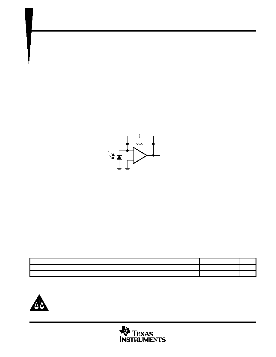
Monolithic Silicon IC Containing
Photodiode, Operational Amplifier, and
Feedback Components
D
Converts Light Intensity to Output Voltage
D
High Irradiance Responsivity Typically
80 mV/(
µ
W/cm
2
) at
p
= 880 nm (TSL250)
D
Compact 3-Leaded Clear Plastic Package
D
Low Dark (Offset) Voltage . . . 10 mV
Max at 25
∞
C, V
DD
= 5 V
D
Single-Supply Operation
D
Wide Supply-Voltage Range . . . 3 V to 9 V
D
Low Supply Current . . . 800
µ
A Typical at
V
DD
= 5 V
D
Advanced LinCMOS
TM
Technology
description
The TSL250, TSL251, and TSL252 are light-to-voltage optical sensors, each combining a photodiode and a
transimpedance amplifier (feedback resistor = 16 M
, 8 M
, and 2 M
respectively) on a single monolithic IC.
The output voltage is directly proportional to the light intensity (irradiance) on the photodiode. These devices
utilize Texas Instruments silicon-gate LinCMOS
TM
technology, which provides improved amplifier offset-voltage
stability and low power consumption.
functional block diagram
Voltage
Output
+
≠
absolute maximum ratings over operating free-air temperature range (unless otherwise noted)
Supply voltage, V
DD
(see Note 1)
10 V
. . . . . . . . . . . . . . . . . . . . . . . . . . . . . . . . . . . . . . . . . . . . . . . . . . . . . . . . . . . .
Output current, I
O
±
10 mA
. . . . . . . . . . . . . . . . . . . . . . . . . . . . . . . . . . . . . . . . . . . . . . . . . . . . . . . . . . . . . . . . . . . . . . .
Duration of short-circuit current at (or below) 25
∞
C (see Note 2)
5 s
. . . . . . . . . . . . . . . . . . . . . . . . . . . . . . . . . . .
Operating free-air temperature range, T
A
≠ 25
∞
C to 85
∞
C
. . . . . . . . . . . . . . . . . . . . . . . . . . . . . . . . . . . . . . . . . . . .
Storage temperature range, T
stg
≠ 25
∞
C to 85
∞
C
. . . . . . . . . . . . . . . . . . . . . . . . . . . . . . . . . . . . . . . . . . . . . . . . . . . .
Lead temperature 1,6 mm (1/16 inch) from case for 10 seconds
240
∞
C
. . . . . . . . . . . . . . . . . . . . . . . . . . . . . . .
Stresses beyond those listed under "absolute maximum ratings" may cause permanent damage to the device. These are stress ratings only, and
functional operation of the device at these or any other conditions beyond those indicated under "recommended operating conditions" is not
implied. Exposure to absolute-maximum-rated conditions for extended periods may affect device reliability.
NOTES:
1. All voltages are with respect to GND.
2. Output may be shorted to supply.
recommended operating conditions
MIN
NOM
MAX
UNIT
Supply voltage, VDD
3
5
9
V
Operating free-air temperature, TA
0
70
∞
C
Please be aware that an important notice concerning availability, standard warranty, and use in critical applications of
Texas Instruments semiconductor products and disclaimers thereto appears at the end of this data sheet.
LinCMOS is a trademark of Texas Instruments Incorporated.
Copyright
©
1995, Texas Instruments Incorporated
PRODUCTION DATA information is current as of publication date.
Products conform to specifications per the terms of Texas Instruments
standard warranty. Production processing does not necessarily include
testing of all parameters.

TSL250, TSL251, TSL252
LIGHT-TO-VOLTAGE OPTICAL SENSORS
SOES004C ≠ AUGUST 1991 ≠ REVISED NOVEMBER 1995
2
POST OFFICE BOX 655303
∑
DALLAS, TEXAS 75265
electrical characteristics at V
DD
= 5 V, T
A
= 25
∞
C,
p = 880 nm, R
L
= 10 k
(unless otherwise noted)
(see Note 3)
PARAMETER
TEST
TSL250
TSL251
TSL252
UNIT
PARAMETER
CONDITIONS
MIN
TYP
MAX
MIN
TYP
MAX
MIN
TYP
MAX
UNIT
VD
Dark voltage
Ee = 0
3
10
3
10
3
10
mV
VOM
Maximum output
voltage swing
Ee = 2 mW/cm2
3.1
3.5
3.1
3.5
3.1
3.5
V
Ee = 25
µ
W/cm2
1
2
3
VO
Output voltage
Ee = 45
µ
W/cm2
1
2
3
V
Ee = 285
µ
W/cm2
1
2
3
Temperature
Ee = 25
µ
W/cm2,
TA = 0
∞
C to 70
∞
C
±
1
vo
Tem erature
coefficient of
output voltage
Ee = 45
µ
W/cm2,
TA = 0
∞
C to 70
∞
C
±
1
mV/
∞
C
(VO)
Ee = 285
µ
W/cm2,
TA = 0
∞
C to 70
∞
C
±
1
Ne
Irradiance
responsivity
See Note 4
80
45
7
mV/(
µ
W/cm2)
Ee = 25
µ
W/cm2
900
1600
IDD
Supply current
Ee = 45
µ
W/cm2
900
1600
µ
A
Ee = 285
µ
W/cm2
900
1600
NOTES:
3. The input irradiance Ee is supplied by a GaAlAs infrared-emitting diode with
p = 880 nm.
4. Irradiance responsivity is characterized over the range VO = 0.05 to 3 V.
operating characteristics at T
A
= 25
∞
C (see Figure 1)
PARAMETER
TEST CONDITIONS
TSL250
TSL251
TSL252
UNIT
PARAMETER
TEST CONDITIONS
MIN
TYP
MAX
MIN
TYP
MAX
MIN
TYP
MAX
UNIT
tr
Output pulse rise time
VDD = 5 V,
p = 880 nm
360
90
7
µ
s
tf
Output pulse fall time
VDD = 5 V,
p = 880 nm
360
90
7
µ
s
Vn Output noise voltage
VDD = 5 V,
f = 20 Hz
0.6
0.5
0.4
µ
V/
Hz
PARAMETER MEASUREMENT INFORMATION
VOLTAGE WAVEFORM
TEST CIRCUIT
Input
Ee
10%
90%
Output
(see Note B)
tr
TSL25x
RL
VDD
2
1
3
+
≠
Output
Pulse
Generator
IRED
(see Note A)
tf
90%
10%
NOTES: A. The input irradiance is supplied by a pulsed GaAlAs infrared-emitting diode with the following characteristics:
p = 880 nm,
tr < 1
µ
s, tf < 1
µ
s.
B. The output waveform is monitored on an oscilloscope with the following characteristics: tr < 100 ns, Zi
1 MHz, Ci
20 pF.
Figure 1. Switching Times
TSL250, TSL251, TSL252
LIGHT-TO-VOLTAGE OPTICAL SENSORS
SOES004C ≠ AUGUST 1991 ≠ REVISED NOVEMBER 1995
5
POST OFFICE BOX 655303
∑
DALLAS, TEXAS 75265
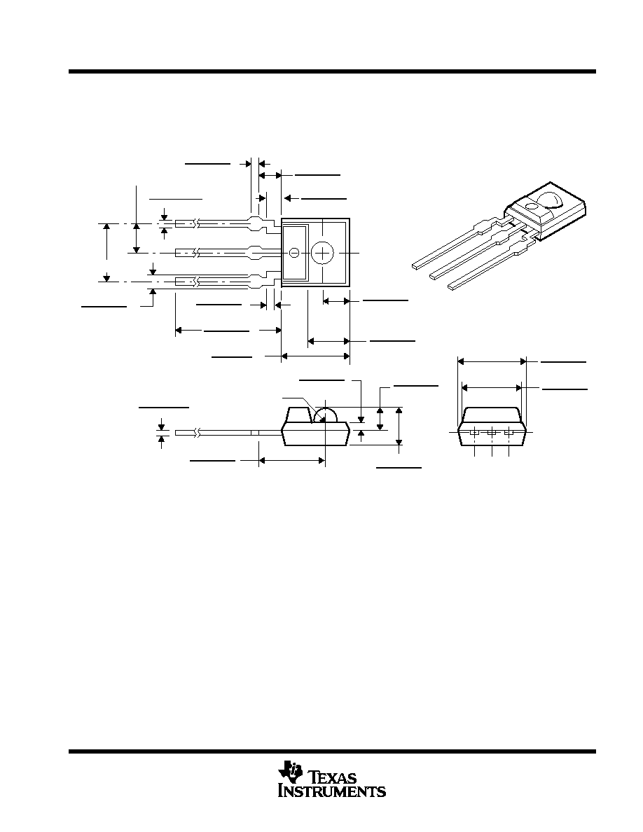
APPLICATION INFORMATION
The photodiode/amplifier chip is packaged in a clear plastic three-leaded package. The integrated photodiode active
area is typically 1,0 mm
2
(0.0016 in
2
) for TSL250, 0,5 mm
2
(0.00078 in
2
) for the TSL251, and 0,26 mm
2
(0.0004 in
2
)
for the TSL252.
2,25 (0.089)
1,75 (0.069)
0,75 (0.030)
0,65 (0.026)
0,635 (0.025)
0,4 (0.016)
2,0 (0.079) T.P.
4,0 (0.157) T.P.
1
2
3
15,7 (0.619)
13,2 (0.520)
0,86 (0.034)
0,46 (0.018)
2,05 (0.081)
1,55 (0.061)
3,05 (0.120)
2,55 (0.100)
4,8 (0.189)
4,4 (0.173)
0,75 (0.030) R
0,85 (0.033)
0,35 (0.014)
2,74 (0.108)
2,34 (0.092)
5,05 (0.199)
4,55 (0.179)
4,85 (0.191)
4,35 (0.171)
4,35 (0.171)
3,85 (0.152)
Pin 1
GND
Pin 2
VDD
Pin 3
OUT
1
2
3
0,51 (0.02)
0,385 (0.015)
1,25 (0.049)
0,75 (0.029)
1,75 (0.069)
1,25 (0.049)
0,65 (0.026)
0,55 (0.022)
True position when unit is installed.
NOTES: A. All linear dimensions are in millimeters (inches).
B. This drawing is subject to change without notice.
Figure 7. Mechanical Data

