 | –≠–ª–µ–∫—Ç—Ä–æ–Ω–Ω—ã–π –∫–æ–º–ø–æ–Ω–µ–Ω—Ç: UCC28089 | –°–∫–∞—á–∞—Ç—å:  PDF PDF  ZIP ZIP |
UCC28089
SLUS623 - SEPTEMBER 2004
PRIMARY-SIDE PUSH-PULL OSCILLATOR
WITH DEAD-TIME CONTROL
1
www.ti.com
FEATURES
D
Push-Pull Oscillator With Programmable
Deadtime
D
High-Current Totem-Pole Dual Output Stage
Drives Push-Pull Configuration with 1-A Sink
and 0.5-A Source Capability
D
Can be Used in Push-Pull, Half-Bridge, or
Full-Bridge Topologies
D
Oscillator Synchronization Output
D
Low Start-Up Current of 130
µ
A and 1.4-mA
Typical Run Current
D
Over-Current Shutdown
D
Digitally Controlled Over-Current/Retry
Feature
D
Undervoltage Lockout With Hysteresis
APPLICATIONS
D
High Efficiency Cascaded Converters
D
Inverters
D
Electronic Ballasts
D
Uninterruptable Power Supplies (UPS)
D
AC or DC Links
DESCRIPTION
The UCC28089 is a versatile BiCMOS controller for
dc-to-dc or off-line fixed-frequency switching power
supplies. The UCC28089 has dual alternating output
stages in dual-alternating push-pull configuration. Both
outputs switch at half the oscillator frequency using a
toggle flip-flop and duty cycle is limited to less than 50%.
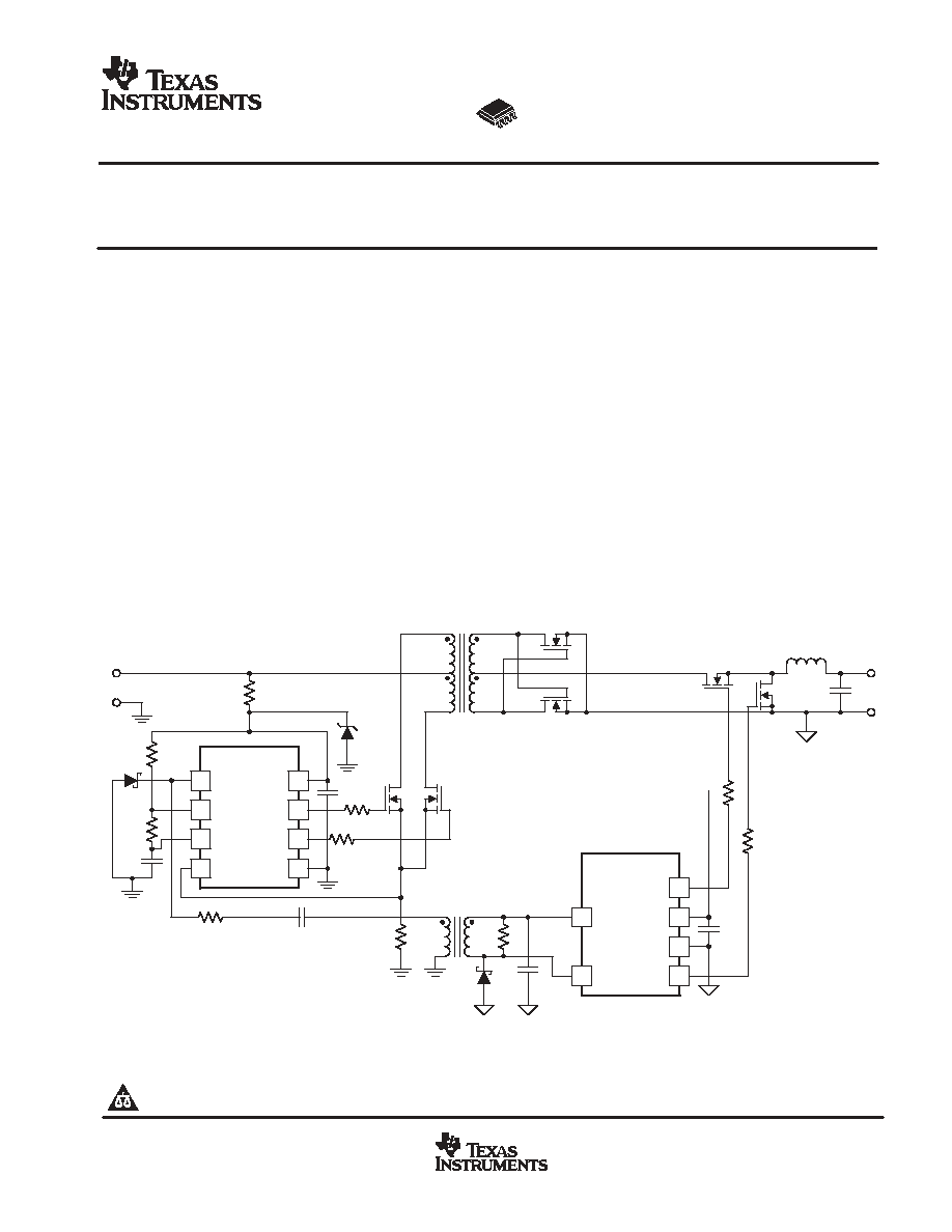
TYPICAL APPLICATION
2
1
4
3
7
8
5
6
UCC28089
SYNC
DIS
CT
CS
VDD
OUTA
OUTB
GND
+
-
2
4
18
UCC2540
REF
SYNCIN
G1
15
16
14
VDD
PGND
G2
-
BIAS
UDG-04112
RA
RB
CT
VIN = 48 V
VO = 1.2 V
+
Please be aware that an important notice concerning availability, standard warranty, and use in critical applications of Texas Instruments
semiconductor products and disclaimers thereto appears at the end of this data sheet.
PRODUCTION DATA information is current as of publication date.
Products conform to specifications per the terms of Texas Instruments
standard warranty. Production processing does not necessarily include
testing of all parameters.

UCC28089
SLUS623 - SEPTEMBER 2004
2
www.ti.com
DESCRIPTION (CONTINUED)
The UCC28089 is optimized for use as the primary-side companion controller for a cascaded converter that has
secondary-side control. The device incorporates dead-time programming. The synchronization output also
provides dead-time information. The retry and soft-start duration scales with the oscillator clock frequency for
high performance fault recovery.
The UCC28089 also provides primary side under-voltage protection (UVLO), and over-current protection. Both
the soft start and retry after fault durations scale with oscillator frequency for high performance. The turn-on/off
UVLO thresholds are 10.5 V/8.0 V.
ORDERING INFORMATION
TEMPERATURE RANGE
PACKAGED DEVICES
{
TEMPERATURE RANGE
TA = TJ
SOIC-8 (D)
SON-8 (DRB)
}
-40
∞
C to 105
∞
C
UCC28089D
UCC28089DRB
D (SOIC-8) and DRB (SON-8) packages are available taped and reeled. Add R suffix to device type (e.g. UCC28089DR or UCC28089DRBR)
to order quantities of 2,500 devices per reel (for D), and 1,000 devices per reel (for DRB).
Contact factory through TI sales for the availability of this package. Target availability is October 2004.
CONNECTION DIAGRAM
1
2
3
4
8
7
6
5
SYNC
DIS
CT
CS
VDD
OUTA
OUTB
GND
D PACKAGE (SOIC-8)
(TOP VIEW)
8
7
6
5
SYNC
DIS
CT
CS
VDD
OUTA
OUTB
GND
1
2
3
4
DRB PACKAGE (SON-8)
(TOP VIEW)
UCC28089
SLUS623 - SEPTEMBER 2004
3
www.ti.com
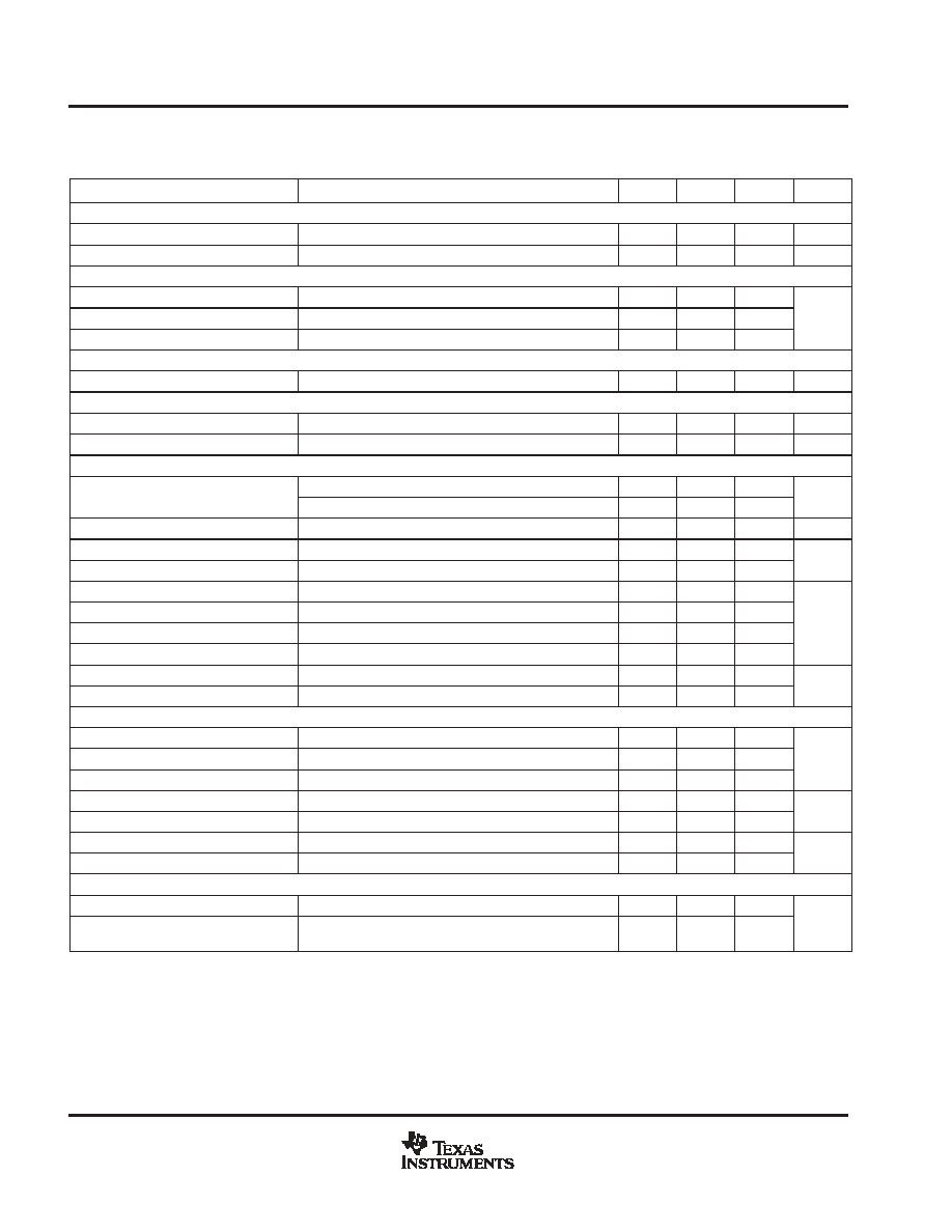
ABSOLUTE MAXIMUM RATINGS
over operating free-air temperature (unless otherwise noted)
}
PARAMETER
SYMBOL
RATING
UNITS
Supply voltage (IDD < 10 mA)
VDD
15
V
Supply current
IDD
20
mA
OUTA/OUTB sink current (peak)
IOUT(sink)
1.0
A
OUTA/OUTB source current (peak)
IOUT(source)
-0.5
A
SYNC sink current (peak)
50
mA
SYNC source current (peak)
-50
mA
Analog inputs (DIS, CT, CS)
-0.3 to VDD + 0.3, not to exceed 5
V
Power dissipation at TA = 25
∞
C (D package)
650
mW
Power dissipation at TA = 25
∞
C (DRB package)
TBD
mW
Junction operating temperature
TJ
-55 to 150
Storage temperature
Tstg
-65 to 150
oC
Lead temperature (soldering, 10 sec.)
Tsol
+300
oC
Stresses beyond those listed under "absolute maximum ratings" may cause permanent damage to the device. These are stress ratings only, and
functional operation of the device at these or any other conditions beyond those indicated under "recommended operating conditions" is not
implied. Exposure to absolute-maximum-rated conditions for extended periods may affect device reliability.
All voltages are with respect to GND. Currents are positive into, negative out of the specified terminal. Consult Packaging Section of the Databook
for thermal limitations and considerations of packages.
RECOMMENDED OPERATION CONDITIONS
Parameter
Symbol
MIN
TYP
MAX
UNITS
Supply voltage (IDD < 10 mA)
VDD
8.5
14
V
SYNC sink current (peak)
0
10
25
mA
SYNC source current (peak)
-25
-10
0
mA
Analog inputs (DIS, CT, CS)
0
4
V
Timing capacitor range
CT
100
100,000
pF
Timing charge resistor range
RA
32
750
k
Discharge resistor range
RB
0
250
k
Timing charge current
ICHG(RA+RB)
10
300
mA
Switching Frequency
fSW
1000
kHz
Junction temperature
TJ
-40
105
∞
C
UCC28089
SLUS623 - SEPTEMBER 2004
4
www.ti.com
ELECTRICAL CHARACTERISTICS:
TA = -40
∞
C to 105
∞
C for UCC28089, VDD = 9 V (see Note 1), 1
µ
F capacitor from VDD to GND, RA = 110 k
, RB = 182
, CT = 220 pF, TA = TJ,
(unless otherwise noted).
PARAMETER
TEST CONDITION
MIN
TYP
MAX
UNITS
Overall Section
Startup current
VDD < UVLO start threshold (see Note 2)
130
260
µ
A
Operating supply current
CS = 0 V, (see Note 1, Note 2)
1.4
2.0
mA
Undervoltage Lockout
Start threshold
See Note 1
9.5
10.5
11.5
Minimum operating voltage after start
7.4
8.0
8.4
V
Hysteresis
2.1
2.5
2.9
V
Oscillator
Oscillator frequency
2 x OUTx frequency, Measured at output(s)
180
200
220
kHz
Current Sense
Current Shutdown threshold
Resetting current limit
0.650
0.725
0.800
V
CS to output delay
CS from 0 mV to 900 mV
45
100
ns
Output
Dead Time
Measured at OUTA or OUTB
90
100
110
ns
Dead Time
Over temperature
80
125
ns
Minimum duty cycle
CS = 0.9 V
0
%
VOL (OUTA or OUTB)
IOUT = 75 mA
0.5
1
V
VOH (OUTA or OUTB)
IOUT = -35 mA, (VDD ≠ VOUT)
1.0
1.3
V
Output resistance high
TA = 25
∞
C IOUT = -1 mA (see Note 4)
70
80
90
TA = full range IOUT = -1 mA (see Note 4)
40
80
135
Output resistance low
TA = 25
∞
C IOUT = 1 mA (see Note 4)
6.5
7.5
8.5
TA = full range IOUT = 1 mA (see Note 4)
4
7.5
14
tr, Rise Time
CLOAD = 1 nF
28
50
ns
tf, Fall Time
CLOAD = 1 nF
13
30
ns
SYNC
SYNC duration
Measured at SYNC pin
75
95
115
tr, delay
Rising SYNC until falling OUTA or OUTB
0
8.5
30
ns
tf, delay
Falling SYNC until rising OUTA or OUTB
0
14
50
ns
SYNC VOH
ISYNC = -5 mA (VDD ≠ VSYNC)
0.3
1
V
SYNC VOL
ISYNC = 5 mA
0.3
1
V
tr, Rise Time
CLOAD = 100 pF
15
30
ns
tf, Fall Time
CLOAD = 100 pF
15
30
ns
Soft Start & Fault
OUTA/OUTB start delay time
Cycles as measured at CT pin
57
59
62
OUTA/OUTB soft start duration
First output stage cycle to first full output stage cycle,
CS
0.6 V
4
5
7
cycles
NOTES:
1. Set VDD above the start threshold before setting at 9V.
2. Does not include current of the external oscillator network.
3. Ensured by design. Not 100% tested in production.
4. The pullup / pulldown circuits of the driver are bipolar and MOSFET transistors in parallel. The output resisstance is the RDS(ON)
of the MOSFET transistor when the voltage of the driver output is less than the saturation voltage of the bipolar transistor.
UCC28089
SLUS623 - SEPTEMBER 2004
5
www.ti.com
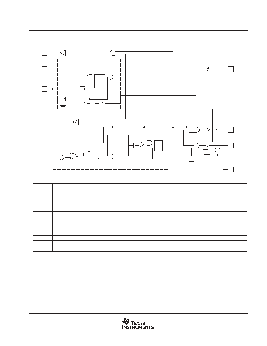
FUNCTIONAL BLOCK DIAGRAM
OUTPUT LOGIC
UCC28089
6
OUTB
7
OUTA
8
VDD
4
CS
2
DIS
1
SYNC
3
CT
5
GND
VDD
UVLO
VDD = 10.5/8.0 V
VDD
OVER
CURRENT
COMP
SS LATCH
0.725 V
SS
COMP
Q
Q
S
R
+
0.2V
56 STEP
START
DELAY
R
GO
7 STEP SOFT-
START RAMP
REF
GO
VDD/5
S
Q
Q
R
CK
VDD/5
VDD/19.6
Q
T
_
Q
SOFT-START & FAULT
OSCILLATOR
UDG-04101
PIN #
NAME
I/O
FUNCTION
1
SYNC
O
Active when OUTA and OUTB are active, logic LO at all other times such as during under-voltage
lock-out and over-current shutdown. When active, SYNC is logic HI (VDD) during the discharge time
of the oscillator and logic LO (GND) at all other times. The pulse occur during the dead time.
2
DIS
I
Separate oscillator timing capacitor discharge pin that allows the dead time to be externally
programmed.
3
CT
I
Oscillator timing capacitor connection.
4
CS
I
Current sense pin. An over current shutdown event is triggered when the voltage of this pin rises
above 0.75 V.
5
GND
-
Ground pin. Analog and digital signals reference this pin and output drivers return current through
this pin
6
OUTB
O
Driver output, capable of sinking 1 A and sourcing 0.5 A. OUTB signal alternates with OUTA.
7
OUTA
O
Driver output, capable of sinking 1 A and sourcing 0.5 A. OUTA signal alternates with OUTB.
8
VDD
I
Power input connection for this device.