 | –≠–ª–µ–∫—Ç—Ä–æ–Ω–Ω—ã–π –∫–æ–º–ø–æ–Ω–µ–Ω—Ç: UCC3305 | –°–∫–∞—á–∞—Ç—å:  PDF PDF  ZIP ZIP |

UCC2305
UCC3305
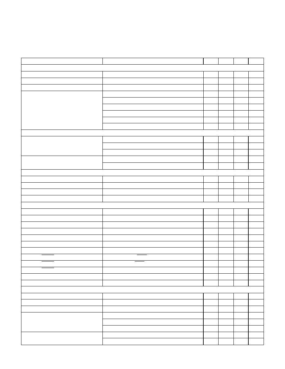
BLOCK DIAGRAM
SLUS297B - SEPTEMBER 1995 - REVISED APRIL 2004
∑
Regulates Lamp Power
∑
Compensates For Lamp
Temperature
∑
Fixed Frequency Operation
∑
Current Mode Control
∑
Overcurrent Protected
∑
Overvoltage Shutdown
∑
Open and Short Protected
∑
High Current FET Drive Output
∑
Operates Over Wide Battery
Voltage Range: 5V to 18V
The UCC3305 integrates all of the functions required to control and drive one
HID lamp. The UCC3305 is tailored to the demanding, fast turn-on requirements
of automobile headlamps, but is also applicable to all other lighting applications
where HID lamps are selected. HID lamps are ideal for any lighting applications
that can benefit from very high efficiency, blue-white light color, small physical
lamp size, and very long life.
The UCC3305 contains a complete current mode pulse width modulator, a lamp
power regulator, lamp temperature compensation, and total fault protection.
Lamp temperature compensation is critical for automobile headlamps, because
without compensation, light output varies dramatically from a cold lamp to one
that is fully warmed up.
The UCC2305 is tested for full performance with ambient temperature
from ≠40
∞
C to +105
∞
C while the UCC3305 is tested with ambient temperature
from 0
∞
C to +70
∞
C. The UCC3305 is available in a 28 pin small-outline, surface
mount plastic package (SOIC).
HID Lamp Controller
FEATURES
DESCRIPTION
UDG-94091-1
application
INFO
available

2
UCC2305
UCC3305
ABSOLUTE MAXIMUM RATINGS
VCC Supply Voltage. . . . . . . . . . . . . . . . . . . . . . . . . . . . . . 8.0V
BOOST Supply Voltage . . . . . . . . . . . . . . . . . . . . . . . . . . 12.0V
PWMOUT Current, Peak
. . . . . . . . . . . . . . . . . . . . . . . . . . . . ±
1.0A
PWMOUT Energy, Capacitive Load . . . . . . . . . . . . . . . . . 5.0
µ
J
Input Voltage, Any Input. . . . . . . . . . . . . . . . . . ≠0.3V to +10.0V
Output Current, QOUT, QOUT, FLT . . . . . . . . . . . . . .
±
10.0mA
Output Current, 5VREF, LPOWER, COMP . . . . . . . . .
±
10.0mA
ISET Current . . . . . . . . . . . . . . . . . . . . . . . . . . . . . . . . . ≠1.0mA
Storage Temperature . . . . . . . . . . . . . . . . . . .
-
65
∞
C to +150
∞
C
Junction Temperature . . . . . . . . . . . . . . . . . . .
-
55
∞
C to +150
∞
C
Lead Temperature . . . . . . . . . . . . . . . . . . . . . . . . . . . . . +300
∞
C
CONNECTION DIAGRAM
ELECTRICAL CHARACTERISTICS
Unless otherwise stated, VCC = 6.6V, ISET = 100k
to GND, ADJ = 100k
to GND,
OSC = 200pF to GND, BAT = 4V, LOADISENSE connected to LPOWER, VOUTSENSE = 0.666V, BOOST = 10.5V, COMP
connected to FB through a 100k
resistor, ≠40
∞
C<T
A
<+105
∞
C for the UCC2305, 0
∞
C<T
A
<+70
∞
C for the UCC3305, and T
A
=T
J
.
PARAMETER
TEST CONDITIONS
MIN.
TYP.
MAX. UNITS
Overall Section
VCC Supply Current
0.1
1.0
mA
BOOST Supply Current
3.0
5.0
mA
BOOST Threshold to PUMP Stop
9.1
9.6
10.2
V
BOOST Threshold to PUMP Start
9.2
9.7
10.3
V
BOOST Threshold to PWMOUT
4.7
5.4
6.1
V
Battery Section
BAT Threshold to PWMOUT Stop
4.7
5.0
5.3
V
BAT Threshold to PWMOUT Start
4.15
4.8
5.0
V
BAT Input Current
BAT = 4V
≠1
1
µ
A
Oscillator & Divider Section
OSC Frequency
80
100
120
kHz
OSC Pull-Up Current
OSC = 1.5V
-
70
-
50
-
40
µ
A
DIVPAUSE Threshold to Pause
1.1
1.5
1.9
V
DIVPAUSE Threshold to Divide
0.8
1.2
1.6
V
DIVPAUSE Input Current
0V < DIVPAUSE < 6V
≠8
≠5
≠1
µ
A
Reference Section
5VREF Voltage
4.85
5.0
5.1
V
ISET Voltage
4.8
4.8
5.2
V
Error Amplifier Section
FB Voltage
2.4
2.5
2.6
V
FB Input Current
≠1
0
1
µ
A
FB Sink Current
VOUTSENSE = 4V, FB = 4V
0.3
1.5
mA
FB Release Delay
VOUTSENSE Step from 4V to 1V
15
30
43
ms
COMP Source Current
FB = 2V, COMP = 4V
≠3.0
≠0.2
mA
COMP Sink Current
FB = 3V, COMP = 1V
0.2
1.0
mA
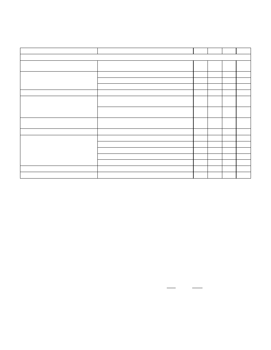
PDIP-28 or SOIC-28 (Top View)
N or DW Package
3
UCC2305
UCC3305
PARAMETER
TEST CONDITIONS
MIN.
TYP.
MAX. UNITS
Load Power Amplifier Section
LOADISENSE Input Current
≠2.5
≠0.1
2.5
µ
A
LPOWER Source Current
LPOWER = 0V
≠8.0
≠0.4
mA
LPOWER Sink Current
LPOWER = 1V
0.4
1.3
mA
LPOWER Voltage
VOUTSENSE = 0.0V
0.32
0.40
0.48
V
VOUTSENSE = 0.45V
0.32
0.40
0.48
V
VOUTSENSE = 0.65V
0.41
0.46
0.51
V
VOUTSENSE = 0.88V
0.43
0.51
0.59
V
VOUTSENSE = 2.0V
0.43
0.51
0.59
V
VOUTSENSE = 0.7V, SLOPEC = 0V
0.29
0.34
0.41
V
Input Current Sense Section
ISENSEIN Threshold
COMP = 5V, WARMUPC = 0V
0.16
0.21
0.28
V
COMP = 5V, WARMUPC = 10V
0.10
0.19
0.27
V
COMP = 1V, WARMUPC = 0V
0.07
0.10
0.2
V
ISENSEIN Bias Current
OSC = 0V
≠15
≠5
≠2
µ
A
OSC = 2V
≠80
≠40
≠15
µ
A
VOUTSENSE Section
VOUTSENSE Threshold to PWMOUT
4.2
5.0
5.2
V
VOUTSENSE Threshold to FB
1.7
1.9
2.1
V
VOUTSENSE Threshold to NOTON
0.035
0.083
0.140
V
VOUTSENSE Input Current
≠1
1
µ
A
OUTPUTS SECTION
PWMOUT High Voltage
I
PWMOUT
= ≠100mA
9.15
10.0
V
PWMOUT Low Voltage
I
PWMOUT
= 100mA
0.3
0.5
V
PUMPOUT High Voltage
I
PUMPOUT
= ≠10mA
5.3
5.8
V
PUMPOUT Low Voltage
I
PUMPOUT
= 10mA
1.0
1.8
V
PUMPOUT Frequency
BOOST = 9.5V
35
50
60
kHz
NOTON High Voltage
I
NOTON
= ≠1mA
5.0
6.3
V
NOTON Low Voltage
I
NOTON
= 1mA
0.1
0.3
V
QOUT, QOUT High Voltage
I
QOUT
= ≠1mA or I
QOUT
= ≠1mA
5.0
6.3
V
QOUT, QOUT Low Voltage
I
QOUT
= 1mA or I
QOUT
= 1mA
0.1
0.45
V
QOUT, QOUT Frequency
150
200
250
Hz
FLT High Voltage
I
FLT
= ≠1mA
6.0
6.3
V
FLT Low Voltage
I
FLT
= 1mA
0.1
0.3
V
Timing Capacitor Section
FLTC Discharge Current
FLTC = 2.5V
35
60
100
nA
FLTC Charge Current
FLTC = 2.5V
≠430
≠300
≠220
nA
FLTC Threshold to FAULT
4.65
4.9
5.1
V
SLOPEC Charge Current
SLOPEC = 0.5V
≠165
≠90
≠60
nA
SLOPEC = 2.2
≠105
≠60
≠40
nA
SLOPEC = 4.2
≠50
≠30
≠10
nA
SLOPEC Voltage
I
SLOPEC
= ≠125nA
1.3
1.5
1.7
V
I
SLOPEC
= ≠50nA
2.8
3.0
3.2
V
ELECTRICAL CHARACTERISTICS (cont.)
Unless otherwise stated, VCC = 6.6V, ISET = 100k
to GND, ADJ = 100k
to GND, OSC = 200pF to GND, BAT = 4V, LOADISENSE connected to LPOWER, VOUTSENSE = 0.666V, BOOST = 10.5V,
COMP connected to FB through a 100k
resistor, ≠40
∞
C<T
A
<+105
∞
C for the UCC2305, 0
∞
C<T
A
<+70
∞
C for the UCC3305, and
T
A
=T
J
.
4
UCC2305
UCC3305
PARAMETER
TEST CONDITIONS
MIN.
TYP.
MAX. UNITS
Timing Capacitor Section (cont.)
SLOPEC Discharge Current
SLOPEC = 2.2V, VCC = 0V, BOOST = 0V,
BYPASS = 8V
40
100
200
nA
WARMUPC Charge Current
WARMUPC = 0V
≠525
≠375
≠275
nA
WARMUPC = 2V
≠525
≠375
≠300
nA
WARMUPC = 6V
≠200
≠120
≠75
nA
WARMUPC Voltage, Charging
I
WARMUPC
= ≠250nA
3.39
3.8
4.1
V
WARMUPC Discharge Current
WARMUPC = 5V, VCC = 0V, BOOST = 0V,
BYPASS = 8V
23
50
126
nA
WARMUPC = 1V, VCC = 0V, BOOST = 0V,
BYPASS = 8V
5
10
34
nA
WARMUPC Voltage, Discharging
I
WARMUPC
= 25nA, VCC = 0V, BOOST = 0V,
BYPASS = 8V
1.5
1.9
2.3
V
ADJ Bias Current
V
ADJ
= 0V
-
38
-
20
-
12
µ
A
WARMUPV Voltage
WARMUPC = 1V
0.05
0.125
0.25
V
WARMUPC = 2V
0.09
1.00
1.5
V
WARMUPC = 3V
2.3
2.48
2.66
V
WARMUPC = 5V
4.5
4.8
5.25
V
WARMUPC = 10V
4.5
4.8
5.25
V
BYPASS Voltage
VCC = 0V
8.8
9.6
V
BYPASS Current
VCC = 0V, BOOST = 0V, BYPASS = 8V
2.5
7
µ
A
ELECTRICAL CHARACTERISTICS (cont.)
Unless otherwise stated, VCC = 6.6V, ISET = 100k
to GND, ADJ = 100k
to GND, OSC = 200pF to GND, BAT = 4V, LOADISENSE connected to LPOWER, VOUTSENSE = 0.666V, BOOST = 10.5V,
COMP connected to FB through a 100k
resistor, ≠40
∞
C<T
A
<+105
∞
C for the UCC2305, 0
∞
C<T
A
<+70
∞
C for the UCC3305, and
T
A
=T
J
.
5VREF: Circuitry in the UCC3305 uses the internal 5V
reference to set currents and thresholds. This reference
can also be used for other functions if required.
ADJ: The ratio of cold lamp peak current to warmed-up
lamp peak current is controlled by the voltage on ADJ. To
select this voltage, connect a resistor from ADJ to GND.
BAT: This input is used to detect excessively high input
voltage and shut down the IC if the input exceeds a pre-
determined level. Connect BAT to a voltage divider
across the input supply. The UCC3305 shuts down when
this input voltage exceeds 5V. To protect the IC in the
event of very high or negative inputs, keep divider imped-
ance higher than 10k.
BOOST: Although the UCC3305 is powered from the
VCC input, most functions of the device operate from a
supply voltage of approximately 10V connected to
BOOST. This 10V supply can be generated by a voltage
doubler using PUMPOUT as an AC signal and external
diodes as switches.
BYPASS: The UCC3305 compensates for lamp tempera-
ture changes by changing the voltage on the SLOPEC
and WARMUPC capacitors. These voltages rise as the
lamp warms up. An internal calculation determines what
power should be applied to the lamp.
When the HID lamp is turned off, power to the lamp and
the controller is removed, leaving these two critical ca-
pacitors charged to specific voltages. Also, with power
off, the lamp will cool down at a controlled rate. It is es-
sential that the two capacitors discharge at a similarly
controlled rate so that if the lamp is restarted before the
lamp is fully cooled, the controller will have an estimate
of new lamp temperature, and can again command the
correct power for the lamp.
Power to control the discharge of these capacitors comes
from energy stored in a large capacitor connected to BY-
PASS. The value of the capacitor required can be esti-
mated assuming a maximum BYPASS current of 5
µ
A, a
discharge time of 60s, and a maximum allowable droop
of 5V by:
C = I
t
V
= 5 A
60s
5V
= 60 F
∑
∑
µ
µ
COMP: Differences between commanded lamp power
and desired lamp power are amplified by an error ampli-
fier. This amplifier senses the difference between the
voltage at FB and 2.5V, and drives COMP with an ampli-
fied error voltage. A capacitor is normally connected from
COMP to FB to compensate the overall feedback loop so
that the system will be stable.
PIN DESCRIPTIONS

5
UCC2305
UCC3305
DIVPAUSE: The QOUT and QOUT outputs can be used
to switch lamp polarity in an AC ballast. It is important to
stop polarity switching when the lamp is being lit, so that
the arc across the electrodes can form in the correct
place. Pulling high on DIVPAUSE stops the internal di-
vider which generates the QOUT and QOUT signals, and
thereby freezes the QOUT and QOUT signals.
To stop the divider when the lamp is being lit and start af-
ter the lamp has lit, connect a resistor from NOTON to
DIVPAUSE and a capacitor from DIVPAUSE to GND.
FLTC: The voltage on VOUTSENSE is proportional to
lamp voltage. If that voltage is too high or too low, the
lamp is either open, shorted, or not yet running. During
normal operation, there is a capacitor connected to
FLTC, and this capacitor is discharged to 0V by a current
source inside the UCC3305.
The UCC3305 monitors the voltage on VOUTSENSE
and compares it to an internal 83mV lower threshold and
a 2V upper threshold. If the voltage is outside this win-
dow, then the IC will pull up on FLTC with a current of ap-
proximately 250nA. If the fault remains long enough to
charge the external FLTC capacitor over 5V, the control-
ler declares a catastrophic fault and shuts the IC down.
The IC will stay shut down until power is removed from
BOOST.
If the fault clears before the FLTC capacitor reaches 5V,
the capacitor discharges down to 0V. This discharge cur-
rent is approximately 50nA, representing a five times lon-
ger discharge rate than charge rate.
FLT: If the voltage on the FLTC pin exceeds 5V, indicat-
ing a severe fault, then a latch in the UCC3305 sets and
PWM drive is halted. In addition, the FLT output goes
high to VCC, indicating a serious system fault.
FB: Differences between commanded lamp power and
desired lamp power are amplified by an error amplifier.
This amplifier senses the difference between the voltage
at FB and 2.5V, and drives COMP with an amplified error
voltage.
GND: Ground for all functions is through this pin.
ISENSEIN: The power regulating algorithm in the
UCC3305 HID Controller computes a function of lamp
current and lamp voltage and commands the appropriate
battery current to keep lamp power constant. This appro-
priate battery current is sensed by a connection from
I-SENSEIN to a current sense resistor. This current
sensed pulse width modulation scheme is often referred
to as current mode control.
In addition to this current regulation, the UCC3305 con-
tains peak input current limiting. This limiting is set to
0.2V across the ISENSEIN resistor during normal opera-
tion and 0.4V during starting. The transition from starting
to normal operation is accomplished by the rise of the
WARMUPC capacitor.
Current mode control has an advantage over voltage
mode control in that a current mode loop is easier to
compensate. Current mode control has a disadvantage
compared to voltage mode control in that the loop can
enter into chaotic oscillations at high duty cycles. These
chaotic oscillations can be prevented using slope com-
pensation. The UCC3305 contains internal slope com-
pensation in the form of a current proportional to OSC
voltage on ISENSEIN. This current combined with an ex-
ternal resistor from ISENSEIN to the current sense resis-
tor creates a voltage drop proportional to OSC voltage,
which gives slope compensation.
ISET: Many functions inside the UCC3305 require pre-
cise currents to give well controlled performance. These
controlled currents are programmed by a resistor from
ISET to GND. A resistor of 100k programs the IC to nor-
mal operating current. Lower resistor values increase the
internal currents. Some of the functions which are influ-
enced by this resistor are WARMUPC charging and dis-
charging, SLOPEC charging and discharging, FLTC
charging and discharging, and error amplifier bandwidth
LOADISENSE: Just as ISENSEIN is normally connected
to a current sense resistor which monitors battery cur-
rent, LOADISENSE is normally connected to a resistor
which monitors lamp current. Lamp current is then regu-
lated by the controller such that the correct lamp power is
supplied at every lamp temperature, in conjunction with
the lamp voltage sensed by VOUTSENSE.
LPOWER: LOADISENSE directly drives one input of an
op amp in the UCC3305. This amplifier amplifies the dif-
ference between the desired load current and the actual
load current, and generates an output signal on
LPOWER which feeds the error amplifier.
NOTON: While the lamp is in a fault condition, such as
excessively high or low lamp voltage, NOTON is pulled
high to VCC, indicating that the arc is not yet correct.
When the voltage on VOUTSENSE is within the 83mV to
2V window, NOTON is pulled low.
OSC: The fixed frequency PWM in the UCC3305 oper-
ates at the frequency programmed by the OSC pin.
Typically, a a 200pF capacitor from OSC to GND pro-
grams the PWM frequency at 100kHz. In addition, this
programs the charge pump at 50kHz and the QOUT and
QOUT signals at 192Hz. The actual oscillator frequency
is a function of both the capacitor from OSC to GND and
the resistor from ISET to GND.
PUMPOUT: Although the UCC3305 is powered from the
VCC input, most functions of the device operate from a
supply voltage of approximately 10V connected to
BOOST. In normal operation, this 10V supply is gener-
PIN DESCRIPTIONS (cont.)