UCC39161
LOW CURRENT HOT SWAP POWER MANAGER
SLUS410C -- NOVEMBER 1999 -- REVISED FEBRUARY 2000
1
POST OFFICE BOX 655303
∑
DALLAS, TEXAS 75265
D
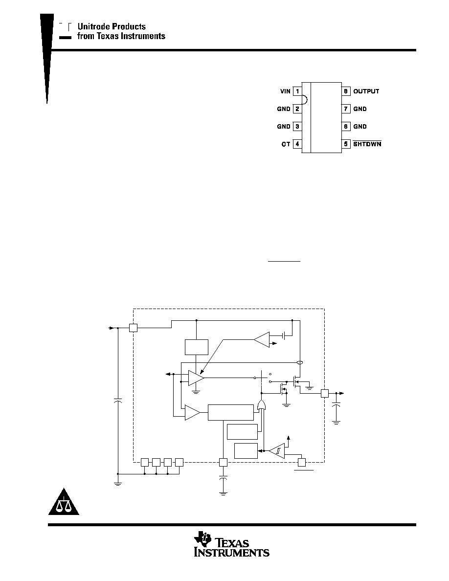
Integrated Circuit Breaker Function
D
Integrated 0.2-W Power FET
D
1mA I
CC
When Disabled
D
Programmable On Time
D
Accurate 0.8-A (MAX) Current
D
Fixed 3% Duty Cycle
D
Unidirectional Switch
D
Thermal Shutdown
description
The UCC39161 low-current hot-swap power manager provides complete power management, hot-swap
capability, and circuit-breaker functions with minimal external components. For most applications, the only
external component required to operate the device, other then supply bypassing, is a timing capacitor that sets
the fault time.
The maximum current level is internally programmed for 0.8 A. While the output current is below 0.8 A, the
internal power MOSFET is switched on at a nominal 220 mW. When the output current exceeds 0.8 A, the
MOSFET transitions from a switch to a constant current source and the fault timer starts charging CT. Once the
fault time is reached, the current shuts off for a time, which equates to a 3% duty cycle.
The UCC39161 also provides unidirectional current flow, emulating a diode in series with the power MOSFET.
The UCC39161 can be put into sleep mode by grounding the SHTDWN pin. In sleep mode, the UCC39161
draws under 5 mA of supply current.
Other features include thermal shutdown and a low thermal-resistance small-outline power package.
block diagram
8
OUTPUT
+
≠
+
OUTPUT
CURRENT SENSE
H=OPEN
REVERSE VOLTAGE
COMPARATOR
30mV
CHARGE
PUMP
POWER
FET
+
≠
+
≠
ON TIME CONTROL
3% DUTY CYCLE
LINEAR
CURRENT
AMPLIFIER
THERMAL
SHUTDOWN
INTERNAL
BIAS
+
≠
1.5V
5
SHTDWN
4
CT
OVER CURRENT
COMPARATOR
2
3
6
7
GND
GND
GND
GND
MAXIMUM
CURRENT
LEVEL
0.8A
4 HEATSINK PINS
LOAD
C
LOAD
C
T
1
VIN
4V to 6V
V
IN
C
IN
UDG-99168
Copyright „ 2000, Texas Instruments Incorporated
PRODUCTION DATA information is current as of publication date.
Products conform to specifications per the terms of Texas Instruments
standard warranty. Production processing does not necessarily include
testing of all parameters.
Please be aware that an important notice concerning availability, standard warranty, and use in critical applications of
Texas Instruments semiconductor products and disclaimers thereto appears at the end of this data sheet.
SOIC 8-PIN
DP PACKAGE
(TOP VIEW)

UCC39161
LOW CURRENT HOT SWAP POWER MANAGER
SLUS410C -- NOVEMBER 1999 -- REVISED FEBRUARY 2000
2
POST OFFICE BOX 655303
∑
DALLAS, TEXAS 75265
absolute maximum ratings over operating free-air temperature (unless otherwise noted)
Input voltage (VIN)
6 V
. . . . . . . . . . . . . . . . . . . . . . . . . . . . . . . . . . . . . . . . . . . . . . . . . . . . . . . . . . . . . . . . . . . . . . . . .
Output current, dc
Self Limiting
. . . . . . . . . . . . . . . . . . . . . . . . . . . . . . . . . . . . . . . . . . . . . . . . . . . . . . . . . . . . . . . . . .
Output current, pulse (less than 100 ns)
20 A
. . . . . . . . . . . . . . . . . . . . . . . . . . . . . . . . . . . . . . . . . . . . . . . . . . . . . .
Storage temperature, T
stg
--65∞C to 150∞C
. . . . . . . . . . . . . . . . . . . . . . . . . . . . . . . . . . . . . . . . . . . . . . . . . . . . . . . .
Junction temperature, T
J
--55
∞C to 150∞C
. . . . . . . . . . . . . . . . . . . . . . . . . . . . . . . . . . . . . . . . . . . . . . . . . . . . . . . . .
Lead temperature (soldering, 10 sec)
300∞C
. . . . . . . . . . . . . . . . . . . . . . . . . . . . . . . . . . . . . . . . . . . . . . . . . . . . . .
Stresses beyond those listed under "absolute maximum ratings" may cause permanent damage to the device. These are stress ratings only, and
functional operation of the device at these or any other conditions beyond those indicated under "recommended operating conditions" is not
implied. Exposure to absolute-maximum-rated conditions for extended periods may affect device reliability.
Currents are positive into, negative out of the specified terminal. Consult Packaging Section of Databook for thermal limitations and
considerations of packages.
electrical characteristics at T
J
= 0∞C to 70∞C, VIN = 5 V, SHTDWN = 2.4 V, T
A
= T
J
(unless otherwise
noted) (see Note 1)
PARAMETER
TEST CONDITIONS
MIN
TYP
MAX
UNITS
Supply Current Section
I
CC
supply current
1.00
2.00
mA
I
CC
supply current (sleep mode)
SHTDWN = 0.2 V
0.50
5
mA
Output Section
Voltage drop
I
OUT
= 0.5 A
0.10
0.16
V
Max current
--1.0
--0.8
--0.6
A
Reverse leakage
VIN = 4.5 V,
V
OUT
= 5 V
6
20
mA
Reverse leakage
VIN = 0 V,
V
OUT
= 5 V
0.50
9
mA
Soft start time
Initial Startup
50
ms
Short circuit response
100
ns
Fault Section
CT charge current
V
CT
= 1.0 V
--45
--36.0
--27
mA
CT discharge current
V
CT
= 1.0 V
0.90
1.0
1.50
mA
Output duty cycle
V
O
= 0 V
2.00
3.00
6.00
%
CT charge threshold
0.4
0.5
0.6
V
CT discharge threshold
1.2
1.4
1.8
V
Thermal shutdown
170
∞C
Thermal hysteresis
10
∞C
Shutdown Section
Shutdown threshold
1.5
3.0
V
Shutdown hysteresis
150
300
mV
Shutdown bias current
SHTDWN = 1.0 V
100
500
nA
NOTE: All voltages are with respect to ground.
UCC39161
LOW CURRENT HOT SWAP POWER MANAGER
SLUS410C -- NOVEMBER 1999 -- REVISED FEBRUARY 2000
3
POST OFFICE BOX 655303
∑
DALLAS, TEXAS 75265
pin description
CT: A capacitor is applied between this pin and ground to set the maximum fault time. The maximum fault time
must be more than the time to charge external capacitance. The maximum fault time is defined as:
TFAULT = 28 ◊ 10
3 ◊ CT
Once the fault time is reached the output will shutdown for a time given by:
TSD = 1 ◊ 10
6 ◊ CT
this results in a 3% duty cycle.
SHTDWN: The IC enters a low-power sleep mode when this pin is low and exits the sleep mode when this pin
is high.
VIN: Input voltage to the circuit breaker, ranging from 4 V to 6 V.
VOUT: Output voltage of the circuit breaker. When switched, the output voltage is approximately:
VOUT = VIN - 220 m ◊ IOUT
5
1
8
4
2
3
6
7
UCC39161
VIN
SHTDWN
GND
GND
GND
GND
CT
OUTPUT
C
T
C
LOAD
C
IN
V
IN
TERMPOWER
BUS
D1
UDG-99167
Figure 1. Typical Application
APPLICATION INFORMATION
protecting the ucc39161 from voltage transients
The parasitic inductance associated with the power distribution can cause a voltage spike at V
IN
if the load
current is suddenly interrupted by the UCC39161. It is important to limit the peak of this spike to less than 6 V
to prevent damage to the UCC39161. This voltage spike can be minimized by:
D
Reducing the power distribution inductance (e.g., twist the positive (+) and negative (--) leads of the power
supply feeding V
IN
, locate the power supply close to the UCC39161 or use a PCB ground plane).
D
Decoupling V
IN
with a capacitor, C
IN
(refer to Figure 1), located close to the VIN pin. This capacitor is
typically less than 1 mF to limit the inrush current.
D
Clamping the voltage at V
IN
below 6 V with a zener diode, D1 (refer to Figure 1), located close to the VIN
pin.
UCC39161
LOW CURRENT HOT SWAP POWER MANAGER
SLUS410C -- NOVEMBER 1999 -- REVISED FEBRUARY 2000
4
POST OFFICE BOX 655303
∑
DALLAS, TEXAS 75265
APPLICATION INFORMATION
safety recommendations
Although the UCC39161 is designed to provide system protection for all fault conditions, all integrated circuits
can ultimately fail short. For this reason, if the UCC39161 is intended for use in safety critical applications where
UL‰ or some other safety rating is required, a redundant safety device such as a fuse should be placed in series
with the device. The UCC39161 prevents the fuse from blowing virtually all fault conditions, increasing system
reliability and reducing maintainence cost, in addition to providing the hot-swap benefits of the device.

IMPORTANT NOTICE
Texas Instruments and its subsidiaries (TI) reserve the right to make changes to their products or to discontinue
any product or service without notice, and advise customers to obtain the latest version of relevant information
to verify, before placing orders, that information being relied on is current and complete. All products are sold
subject to the terms and conditions of sale supplied at the time of order acknowledgment, including those
pertaining to warranty, patent infringement, and limitation of liability.
TI warrants performance of its semiconductor products to the specifications applicable at the time of sale in
accordance with TI's standard warranty. Testing and other quality control techniques are utilized to the extent
TI deems necessary to support this warranty. Specific testing of all parameters of each device is not necessarily
performed, except those mandated by government requirements.
Customers are responsible for their applications using TI components.
In order to minimize risks associated with the customer's applications, adequate design and operating
safeguards must be provided by the customer to minimize inherent or procedural hazards.
TI assumes no liability for applications assistance or customer product design. TI does not warrant or represent
that any license, either express or implied, is granted under any patent right, copyright, mask work right, or other
intellectual property right of TI covering or relating to any combination, machine, or process in which such
semiconductor products or services might be or are used. TI's publication of information regarding any third
party's products or services does not constitute TI's approval, warranty or endorsement thereof.
Copyright
©
2000, Texas Instruments Incorporated