 | –≠–ª–µ–∫—Ç—Ä–æ–Ω–Ω—ã–π –∫–æ–º–ø–æ–Ω–µ–Ω—Ç: UCC5617 | –°–∫–∞—á–∞—Ç—å:  PDF PDF  ZIP ZIP |
18-Line SCSI Terminator (Reverse Disconnect)
UCC5617
FEATURES
∑
Complies with SCSI, SCSI-2,
SCSI-3 and FAST-20 Standards
∑
2pF Channel Capacitance
During Disconnect
∑
50
µ
A Supply Current in
Disconnect Mode
∑ 110
Termination
∑
SCSI Hot Plugging Compliant,
10nA Typical
∑
+
400mA Sinking Current for
Active Negation
∑
-
650mA Sourcing Current for
Termination
∑
Trimmed Impedance to 5%
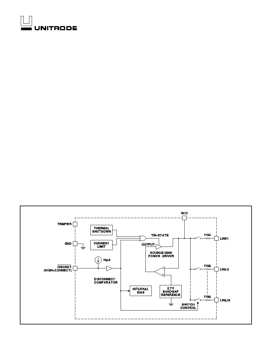
DESCRIPTION
The UCC5617 provides 18 lines of active termination for a SCSI (Small
Computers Systems Interface) parallel bus. The SCSI standard recommends
and Fast-20 (Ultra) requires active termination at both ends of the cable.
Pin for pin compatible with the UC5609, the UCC5617 is ideal for high perfor-
mance 5V SCSI systems, Termpwr 4.0V to 5.25V. During disconnect the sup-
ply current is only 50
µ
A typical, which makes the IC attractive for lower pow-
ered systems.
The UCC5617 is designed with a low channel capacitance of 2pF, which elim-
inates effects on signal integrity from disconnected terminators at interim
points on the bus.
The power amplifier output stage allows the UCC5617 to source full termina-
tion current and sink active negation current when all termination lines are
actively negated.
The UCC5617, as with all Unitrode terminators, is completely hot pluggable
and appears as high impedance at the ter minating channels with
TRMPWR=0V or open.
Internal circuit trimming is utilized, first to trim the 110
impedance, and then
most importantly, to trim the output current as close to the maximum SCSI-3
specification as possible, which maximizes noise margin in fast SCSI opera-
tion.
Other features include thermal shutdown and current limit.
This device is offered in low thermal resistance versions of the industry stan-
dard 28 pin wide body SOIC, TSSOP and PLCC.
4/97
BLOCK DIAGRAM
UDG-96073
Circuit Design Patented
2
UCC5617
ABSOLUTE MAXIMUM RATINGS
Tempwr . . . . . . . . . . . . . . . . . . . . . . . . . . . . . . . . . . . . . . . . . . . . . . . . . . . . . . . . . .+7V
Signal Line Voltage . . . . . . . . . . . . . . . . . . . . . . . . . . . . . . . . . . . . . . . . . . . . .0V to +7V
Regulator Output Current . . . . . . . . . . . . . . . . . . . . . . . . . . . . . . . . . . . . . . . . . . . . .1A
Storage Temperature . . . . . . . . . . . . . . . . . . . . . . . . . . . . . . . . . . . . . .
-
65∞C to
+
150
∞
C
Operating Junction Temperature . . . . . . . . . . . . . . . . . . . . . . . . . . . . .
-
55∞C to
+
150
∞
C
Lead Temperature (Soldering, 10 Seconds) . . . . . . . . . . . . . . . . . . . . . . . . . . . . .300
∞
C
All currents are positive into, negative out of the specified terminal. Consult Packaging
Section of Databook for thermal limitations and considerations of packages.
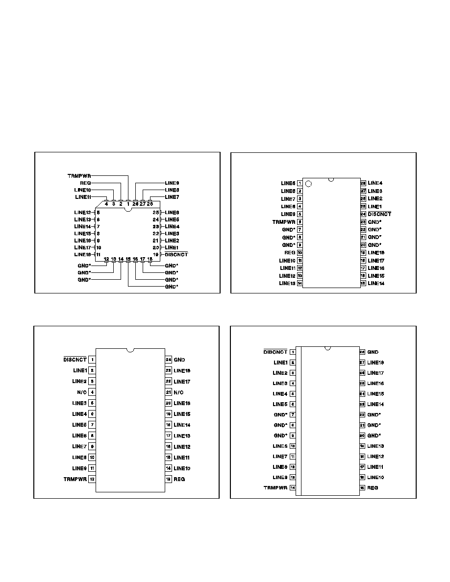
CONNECTION DIAGRAMS
PLCC-28 (Top View)
QP Package
* DWP package pins 12 - 18 serve as both heatsink and signal
ground.
SOIC-28 (Top View)
DWP Package
DIL-24 (Top View)
N Package
* N package for engineering samples only.
* DWP package pin 28 serves as signal ground; pins 7, 8, 9,
20, 21, 22 serve as heatsink/ground.
Note: Drawings are not to scale.
TSSOP-28 (Top View)
PWP Package
* PWP package pin 23 serves as signal ground; pins 7, 8, 9,
20, 21, and 22 serve as heatsink ground.
3
UCC5617
ELECTRICAL CHARACTERISTICS
Unless otherwise stated these specifications apply for T
A
=
0
∞
C to 70
∞
C,
TRMPWR = 4.75V, DISCNCT = 4.75V, T
A
= T
J
.
PARAMETER
TEST CONDITIONS
MIN
TYP
MAX
UNITS
Supply Current Section
Termpwr Supply Current
All termination lines
=
Open
1
2
mA
All termination lines
=
0.2V
420
450
mA
Power Down Mode
DISCNCT
=
0V
50
100
µ
A
Output Section (Termination Lines)
Termination Impedance
(Note 3)
104.5
110
115.5
Output High Voltage
V
TRMPWR
=
4V (Note 1)
2.6
2.8
3
V
Maximum Output Current
V
LINE
=
0.2V, T
J
=
25
∞
C
-
22.1
-
23.3
-
24
mA
V
LINE
=
0.2V
-
20.7
-
23.3
-
24
mA
V
LINE
=
0.2V, TRMPWR = 4V, T
J
= 25∞C (Note 1)
≠21
≠23
≠24
mA
V
LINE
= 0.2V, TRMPWR = 4V (Note 1)
≠20
≠23
≠24
mA
V
LINE
=
0.5V
-
22.4
mA
Output Leakage
DISCNCT
=
0V, TRMPWR
=
0V to 5.25V,
10
400
nA
REG
=
0.2V, V
LINE
=
5.25V
Output Capacitance
DISCNCT
=
2.4V (Note 2)
2
3.5
pF
Regulator Section
Regulator Output Voltage
2.6
2.8
3
V
Drop Out Voltage
All Termination Lines
=
0.2V
0.4
0.8
V
Short Circuit Current
V
REG
=
0V
≠475
-
650
-
850
mA
Sinking Current Capability
V
REG
=
3.5V
200
400
800
mA
Thermal Shutdown
170
∞
C
Thermal Shutdown Hysteresis
10
∞
C
Disconnect Section
Disconnect Threshold
0.8
1.5
2
V
Input Current
DISCNCT
=
0V
-
10
-
30
µ
A
Note 1: Measuring each termination line while other 17 are low (0.2V).
Note 2: Guaranteed by design. Not 100% tested in production.
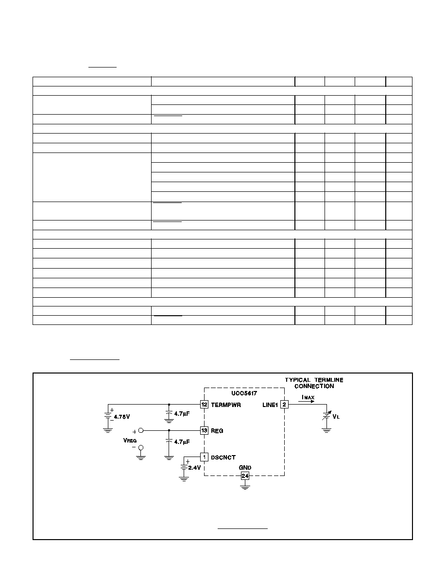
Note 3: Tested by measuring I
OUT
with V
OUT
= 0.2V and V
OUT
with no load, then calculating:
Z =
.
V
OUT
N.L. ≠ 0.2V
I
OUT
at 0.2V
Procedure:
1) Measure V
REG
N.L.
2) Set V
L
= 0.2V; Measure I
MAX
at 0.2V
3) Impedance =
V
REG
N.L. ≠ 0.2V
I
MAX
at 0.2V
Figure 1. Termline Impedance Measurement Circuit
UDG-97108
4
UCC5617
DISCNCT: Taking this pin low causes the 18 channels to
become high impedance and the chip to go into low-power
mode; a high or open state allows the channels to provide
normal termination.
GND: Ground reference for the IC.
LINE 1-18: 110
termination channels.
REG: Output of the internal 2.8V regulator.
TRMPWR: Power for the IC.
PIN DESCRIPTIONS
UNITRODE CORPORATION
7 CONTINENTAL BLVD.
∑
MERRIMACK, NH 03054
TEL. (603) 424-2410
∑
FAX (603) 424-3460
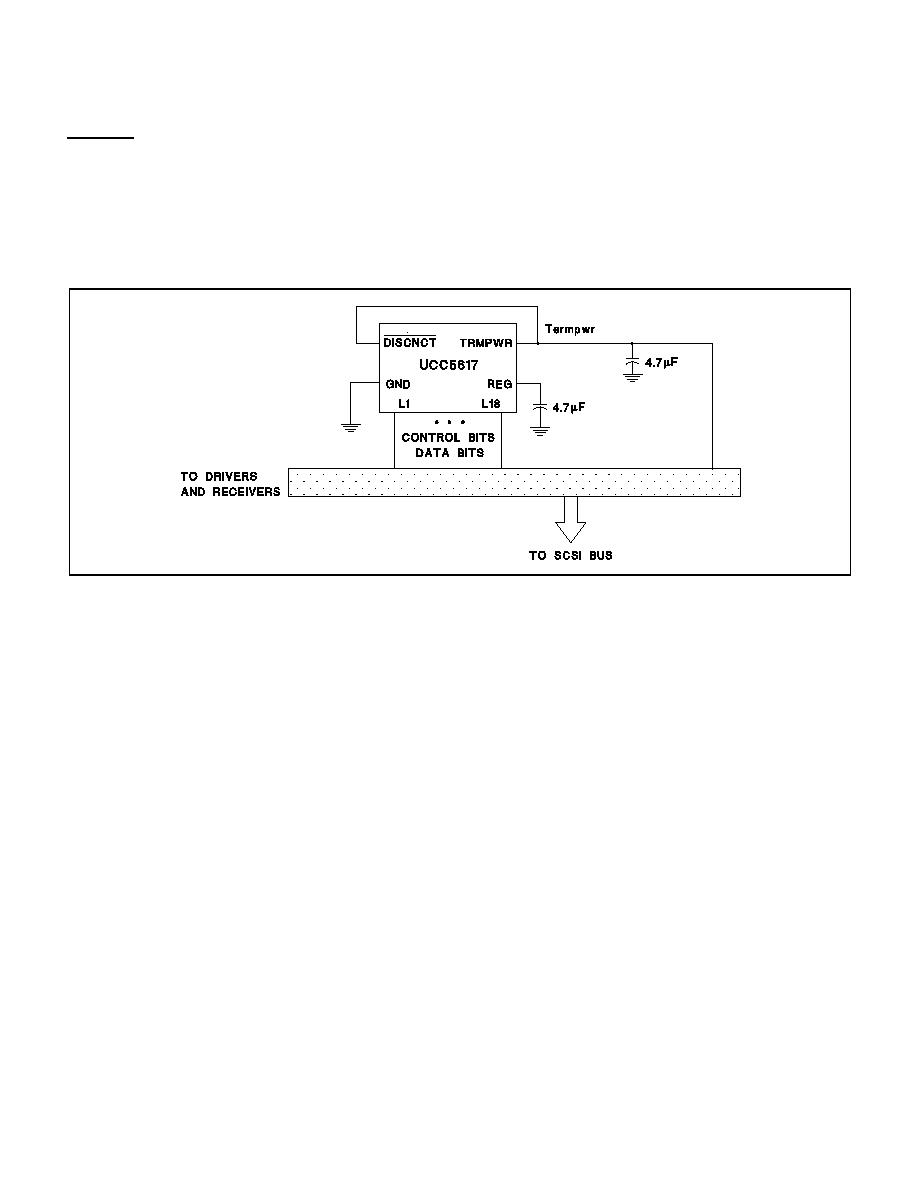
APPLICATION INFORMATION
UDG-96074

IMPORTANT NOTICE
Texas Instruments and its subsidiaries (TI) reserve the right to make changes to their products or to discontinue
any product or service without notice, and advise customers to obtain the latest version of relevant information
to verify, before placing orders, that information being relied on is current and complete. All products are sold
subject to the terms and conditions of sale supplied at the time of order acknowledgement, including those
pertaining to warranty, patent infringement, and limitation of liability.
TI warrants performance of its semiconductor products to the specifications applicable at the time of sale in
accordance with TI's standard warranty. Testing and other quality control techniques are utilized to the extent
TI deems necessary to support this warranty. Specific testing of all parameters of each device is not necessarily
performed, except those mandated by government requirements.
CERTAIN APPLICATIONS USING SEMICONDUCTOR PRODUCTS MAY INVOLVE POTENTIAL RISKS OF
DEATH, PERSONAL INJURY, OR SEVERE PROPERTY OR ENVIRONMENTAL DAMAGE ("CRITICAL
APPLICATIONS"). TI SEMICONDUCTOR PRODUCTS ARE NOT DESIGNED, AUTHORIZED, OR
WARRANTED TO BE SUITABLE FOR USE IN LIFE-SUPPORT DEVICES OR SYSTEMS OR OTHER
CRITICAL APPLICATIONS. INCLUSION OF TI PRODUCTS IN SUCH APPLICATIONS IS UNDERSTOOD TO
BE FULLY AT THE CUSTOMER'S RISK.
In order to minimize risks associated with the customer's applications, adequate design and operating
safeguards must be provided by the customer to minimize inherent or procedural hazards.
TI assumes no liability for applications assistance or customer product design. TI does not warrant or represent
that any license, either express or implied, is granted under any patent right, copyright, mask work right, or other
intellectual property right of TI covering or relating to any combination, machine, or process in which such
semiconductor products or services might be or are used. TI's publication of information regarding any third
party's products or services does not constitute TI's approval, warranty or endorsement thereof.
Copyright
©
1999, Texas Instruments Incorporated