1SV331
2000-09-11 1/3
TOSHIBA Variable Capacitance Diode Silicon Epitaxial Planar Type
1 S V 3 3 1
Useful for VCO/TCXO
∑ Small Package
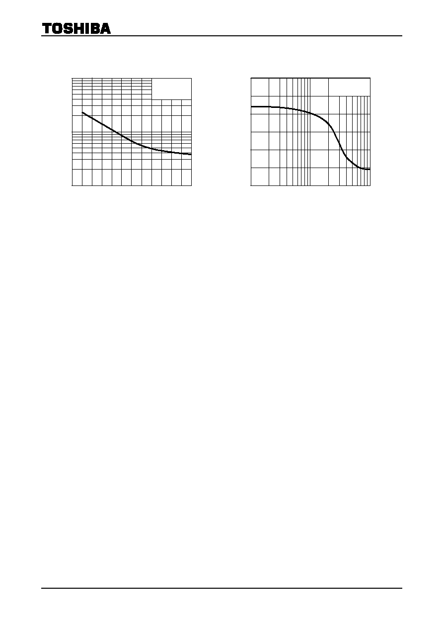
∑ High Capacitance Ratio : C
1V
/C
4V
= 3.75 (typ.)
∑ Low Series Resistance : r
s
= 0.45 (typ.)
Maximum Ratings
(Ta
=
=
=
= 25∞C)
Weight 0.0014 g
Characteristics Symbol
Rating
Unit
Reverse voltage
V
R
10 V
Junction temperature
T
j
125
∞C
Storage temperature range
T
stg
-55~125 ∞C
∑ TOSHIBA is continually working to improve the quality and reliability of its products. Nevertheless, semiconductor devices in general
can malfunction or fail due to their inherent electrical sensitivity and vulnerability to physical stress. It is the responsibility of the
buyer, when utilizing TOSHIBA products, to comply with the standards of safety in making a safe design for the entire system, and
to avoid situations in which a malfunction or failure of such TOSHIBA products could cause loss of human life, bodily injury or
damage to property.
In developing your designs, please ensure that TOSHIBA products are used within specified operating ranges as set forth in the
most recent TOSHIBA products specifications. Also, please keep in mind the precautions and conditions set forth in the "Handling
Guide for Semiconductor Devices," or "TOSHIBA Semiconductor Reliability Handbook" etc..
∑ The TOSHIBA products listed in this document are intended for usage in general electronics applications (computer, personal
equipment, office equipment, measuring equipment, industrial robotics, domestic appliances, etc.). These TOSHIBA products are
neither intended nor warranted for usage in equipment that requires extraordinarily high quality and/or reliability or a malfunction or
failure of which may cause loss of human life or bodily injury ("Unintended Usage"). Unintended Usage include atomic energy
control instruments, airplane or spaceship instruments, transportation instruments, traffic signal instruments, combustion control
instruments, medical instruments, all types of safety devices, etc.. Unintended Usage of TOSHIBA products listed in this document
shall be made at the customer's own risk.
∑ The information contained herein is presented only as a guide for the applications of our products. No responsibility is assumed by
TOSHIBA CORPORATION for any infringements of intellectual property or other rights of the third parties which may result from its
use. No license is granted by implication or otherwise under any intellectual property or other rights of TOSHIBA CORPORATION or
others.
∑ The information contained herein is subject to change without notice.
000707EAA1