TOSHIBA
TOSHIBA CORPORATION
1/6
Discrete Semiconductors
2SK1544
Field Effect Transistor
Silicon N Channel MOS Type (
-MOS III.5)
High Speed, High Current DC-DC Converter,
Relay Drive and Motor Drive Applications
Features
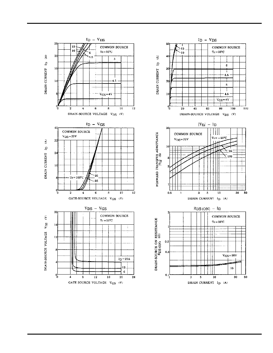
∑ Low Drain-Source ON Resistance
- R
DS(ON)
= 0.15
(Typ.)
∑ High Forward Transfer Admittance
-
Y
fs
= 21S (Typ.)
∑ Low Leakage Current
- I
DSS
= 300
µ
A (Max.) @ V
DS
= 500V
∑ Enhancement-Mode
- V
th
= 1.5 ~ 3.5V @ V
DS
= 10V, I
D
= 1mA
This transistor is an electrostatic sensitive device. Please handle with care.
Absolute Maximum Ratings (Ta = 25
∞
C)
CHARACTERISTIC
SYMBOL
RATING
UNIT
Drain-Source Voltage
V
DSS
500
V
Drain-Gate Voltage (R
GS
= 20k
)
V
DGR
500
V
Gate-Source Voltage
V
GSS
±
30
V
Drain Current
DC
I
D
25
A
Pulse
I
DP
100
Drain Power Dissipation
(Tc = 25
∞
C)
P
D
200
W
Channel Temperature
T
ch
150
∞
C
Storage Temperature Range
T
stg
-55 ~ 150
∞
C
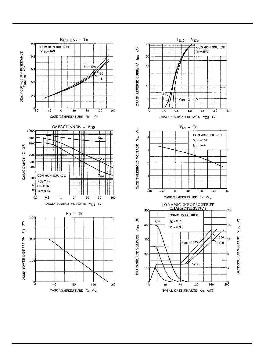
Thermal Characteristics
CHARACTERISTIC
SYMBOL
MAX.
UNIT
Thermal Resistance, Channel to Case
R
th(ch-c)
0.625
∞
C/W
Thermal Resistance, Channel to Ambient
R
th(ch-a)
35.7
∞
C/W
Unit in mm
Industrial Applications
2/6
TOSHIBA CORPORATION
2SK1544
Source-Drain Diode Ratings and Characteristics (Ta = 25
∞
C)
Electrical Characteristics (Ta = 25
∞
C)
CHARACTERISTIC
SYMBOL
TEST CONDITION
MIN.
TYP.
MAX.
UNIT
Gate Leakage Current
I
GSS
V
GS
=
±
25V, V
DS
= 0V
≠
≠
±
100
nA
Drain Cut-off Current
I
DSS
V
DS
= 500V, V
GS
= 0V
≠
≠
300
µ
A
Drain-Source Breakdown Voltage
V
(BR) DSS
I
D
= 10mA, V
GS
= 0V
500
≠
≠
V
Gate Threshold Voltage
V
th
V
DS
= 10V, I
D
= 1mA
1.5
≠
3.5
V
Drain-Source ON Resistance
R
DS (ON)
I
D
= 13A, V
GS
= 10V
≠
0.15
0.20
Forward Transfer Admittance
Y
fs
V
DS
= 10V, I
D
= 13A
10
21
≠
S
Input Capacitance
C
iss
V
DS
= 10V, V
GS
= 0V,
f = 1MHz
≠
3700
5000
pF
Reverse Transfer Capacitance
C
rss
≠
400
750
Output Capacitance
C
oss
≠
920
1300
Switching
Time
Rise Time
t
r
≠
185
370
ns
Turn-on Time
t
on
≠
240
480
Fall Time
t
f
≠
250
500
Turn-off Time
t
off
≠
590
1180
Total Gate Charge
(Gate-Source Plus Gate-Drain)
Q
g
V
DD
= 400V, V
GS
= 10V,
I
D
= 25A
≠
150
250
nC
Gate-Source Charge
Q
gs
≠
70
≠
Gate-Drain ("Miller") Charge
Q
gd
≠
80
≠
CHARACTERISTICS
SYMBOL
TEST CONDITION
MIN.
TYP.
MAX.
UNIT
Continuous Drain Reverse Current
I
DR
≠
≠
≠
25
A
Pulse Drain Reverse Current
I
DRP
≠
≠
≠
100
A
Diode Forward Voltage
V
DSF
I
DR
= 25A, V
GS
= 0V
≠
≠
-1.6
V
Reverse Recovery Time
t
rr
I
DR
= 25A, V
GS
= 0V
dI
DR
/dt = 100A/
µ
s
≠
780
≠
ns
Reverse Recovered Charge
Q
rr
≠
9.8
≠
µ
C