2SK3767
2004-12-10
1
TOSHIBA Field Effect Transistor Silicon N Channel MOS Type (-MOSVI)
2SK3767
Switching Regulator Applications
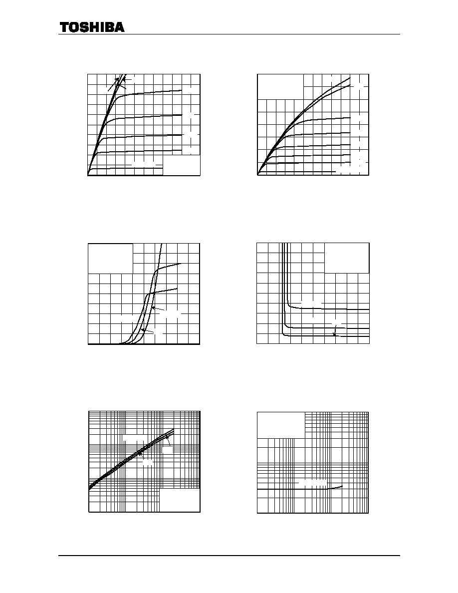
∑ Low drain-source ON resistance: R
DS (ON)
= 3.3 (typ.)
∑ High forward transfer admittance: |Y
fs
| = 1.6S (typ.)
∑ Low leakage current: I
DSS
= 100A (V
DS
= 600 V)
∑ Enhancement mode: V
th
= 2.0 to 4.0 V (V
DS
= 10 V, I
D
= 1 mA)
Maximum Ratings
(Ta
=
25∞C)
Characteristics Symbol
Rating
Unit
Drain-source voltage
V
DSS
600 V
Drain-gate voltage (R
GS
= 20 k) V
DGR
600 V
Gate-source voltage
V
GSS
±30 V
DC (Note
1)
I
D
2
Drain current
Pulse (Note 1)
I
DP
5
A
Drain power dissipation (Tc
= 25∞C)
P
D
25 W
Single pulse avalanche energy
(Note
2)
E
AS
93 mJ
Avalanche current
I
AR
2 A
Repetitive avalanche energy (Note 3)
E
AR
4
mJ
Channel temperature
T
ch
150
∞C
Storage temperature range
T
stg
-55~150 ∞C
Thermal Characteristics
Characteristics Symbol
Max
Unit
Thermal resistance, channel to case
R
th (ch-c)
5.0
∞C/W
Thermal resistance, channel to ambient
R
th (ch-a)
62.5
∞C/W
Note 1: Ensure that the channel temperature does not exceed 150.
Note 2: V
DD
= 90 V, T
ch
= 25∞Cinitial, L = 41mH, R
G
= 25 , I
AR
= 2 A
Note 3: Repetitive rating: pulse width limited by maximum channel temperature
This transistor is an electrostatic-sensitive device. Please handle with caution.
Unit: mm
1: Gate
2: Drain
3: Source
JEDEC
JEITA SC-67
TOSHIBA 2-10U1B
Weight : 1.7 g (typ.)
1
3
2

2SK3767
2004-12-10
2
Electrical Characteristics
(Ta
=
25∞C)
Characteristics Symbol Test
Condition Min
Typ.
Max
Unit
Gate leakage current
I
GSS
V
GS
= ±25 V, V
DS
= 0 V
±10
µA
Gate-source breakdown voltage
V
(BR) GSS
I
G
= ±10 µA, V
DS
= 0 V
±30
V
Drain cut-off current
I
DSS
V
DS
= 600 V, V
GS
= 0 V
100 µA
Drain-source breakdown voltage
V
(BR) DSS
I
D
= 10 mA, V
GS
= 0 V
600
V
Gate threshold voltage
V
th
V
DS
= 10 V, I
D
= 1 mA
2.0
4.0 V
Drain-source ON resistance
R
DS (ON)
V
GS
= 10 V, I
D
= 1 A
3.3 4.5
Forward transfer admittance
Y
fs
V
DS
= 10 V, I
D
= 1 A
0.8
1.6
S
Input capacitance
C
iss
320
Reverse transfer capacitance
C
rss
30
Output capacitance
C
oss
V
DS
= 10 V, V
GS
= 0 V, f = 1 MHz
100
pF
Rise time
t
r
15
Turn-on time
t
on
55
Fall time
t
f
20
Switching time
Turn-off time
t
off
80
ns
Total gate charge
Q
g
9
Gate-source charge
Q
gs
5
Gate-drain charge
Q
gd
V
DD
- 400 V, V
GS
= 10 V, I
D
= 2A
4
nC
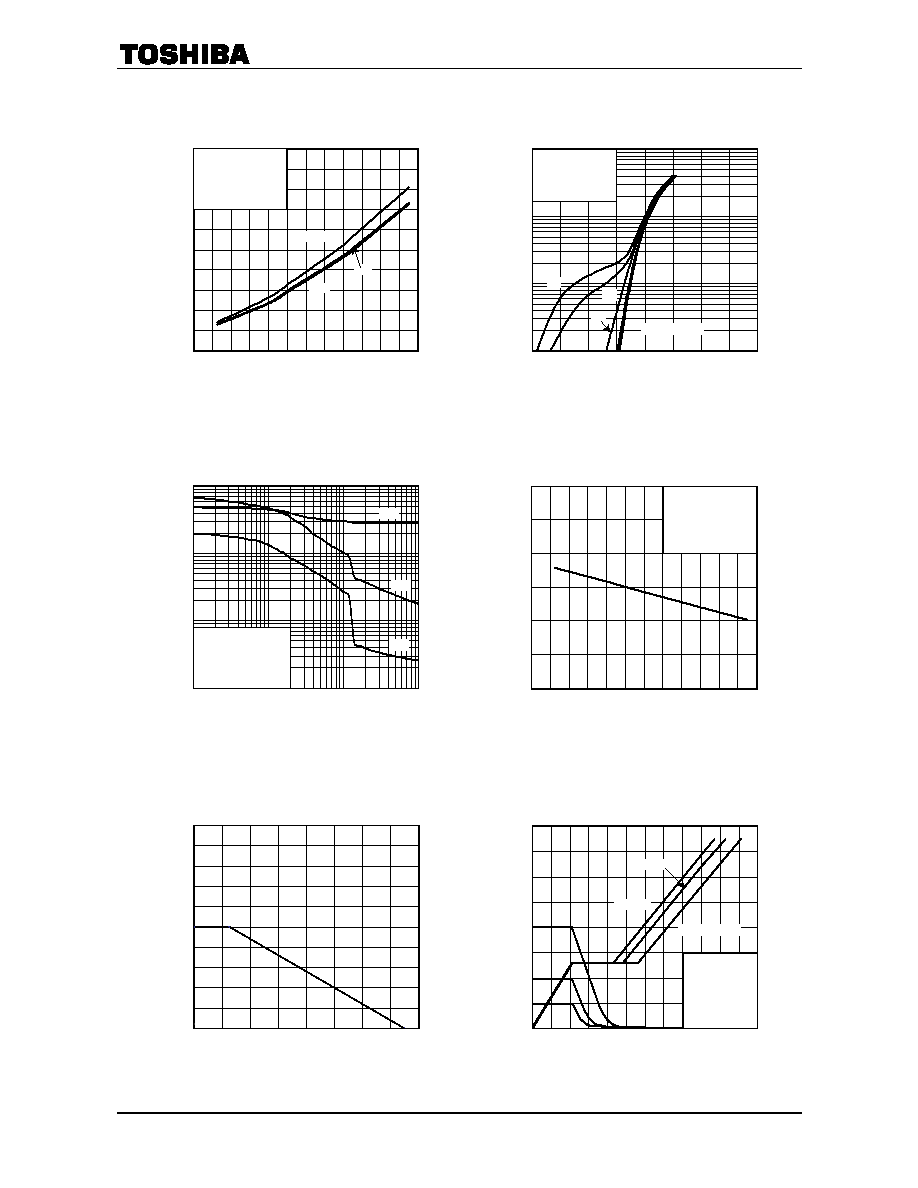
Source-Drain Ratings and Characteristics
(Ta
=
25∞C)
Characteristics Symbol
Test
Condition
Min
Typ.
Max
Unit
Continuous drain reverse current (Note 1)
I
DR
2 A
Pulse drain reverse current (Note 1)
I
DRP
5 A
Forward voltage (diode)
V
DSF
I
DR
= 2 A, V
GS
= 0 V
-1.7
V
Reverse recovery time
t
rr
1000 ns
Reverse recovery charge
Q
rr
I
DR
= 2 A, V
GS
= 0 V,
dI
DR
/dt
= 100 A/µs
3.5
µC
Marking
10
V
I
D
= 1A
Output
Duty <= 1%, t
w
= 10 µs
R
L
=
0 V
V
GS
V
DD
- 200 V
50
200
Lot No.
A line indicates
lead (Pb)-free package or
lead (Pb)-free finish.
K3767
Part No. (or abbreviation code)

2SK3767
2004-12-10
5
-15 V
15
V
TEST CIRCUIT
WAVE FORM
I
AR
B
VDSS
V
DD
V
DS
R
G
= 25
V
DD
= 90 V, L = 41mH
-
=
VDD
BVDSS
BVDSS
2
I
L
2
1
AS
160
120
80
40
0
25 50 75 100 125 150
Channel temperature (initial) T
ch
(∞C)
E
AS
≠ T
ch
Av
a
l
a
n
c
he
e
nerg
y
E
AS
(
m
J
)
200
Darin-source voltage V
DS
(V)
Safe operating area
Single nonrepetitive pulse
Tc=25
Curves must be derated linearly with
increase in temperature.
ID max (PULSED) *
ID max (CONTINUOUS) *
DC OPERATION
Tc
= 25∞C
100
µs *
1 ms *
VDSS max
D
r
a
i
n
c
u
rr
ent
I
D
(A)
100
10
1
0.1
0.01
1000
100
10
1
0.01
0.1
10
0.001
10
100
1 10
100
1 10
0.2
0.1
0.01
r
th
≠ t
w
Pulse width t
w
(s)
N
o
r
m
aliz
ed
t
r
an
s
i
e
n
t
t
h
e
r
m
a
l
i
m
peda
nc
e
r
th (
t
)
/R
th (c
h-c
)
Duty=0.5
SINGLE PULSE
0.003
0.03
1
0.02
0.05
T
PDM
t
Duty
= t/T
Rth (ch-c) = 5/W
3
0.3