 | –≠–ª–µ–∫—Ç—Ä–æ–Ω–Ω—ã–π –∫–æ–º–ø–æ–Ω–µ–Ω—Ç: GT8G132 | –°–∫–∞—á–∞—Ç—å:  PDF PDF  ZIP ZIP |

GT8G132
2002-05-17
1
TOSHIBA Insulated Gate Bipolar Transistor Silicon N Channel IGBT
GT8G132
Strobe Flash Applications
∑
Supplied in compact and thin package requires only a small
mounting area
∑
5th generation (trench gate structure) IGBT
∑
Enhancement-mode
∑
4-V gate drive voltage: V
GE
= 4.0 V (min) (@I
C
= 150 A)
∑
Peak collector current: I
C
= 150 A (max)
Maximum Ratings
(Ta
=
=
=
=
25∞C)
Characteristics Symbol
Rating
Unit
Collector-emitter voltage
V
CES
400 V
DC V
GES
±
6
Gate-emitter voltage
Pulse V
GES
±
8
V
DC I
C
8
Collector current
1 ms
I
CP
150
A
Collector power dissipation
(Note 1)
P
C
1.1
W
Junction temperature
T
j
150 ∞C
Storage temperature range
T
stg
-
55~150 ∞C
Note 1: Drive operation: Mount on glass epoxy board [1 inch
2
◊
1.5 t]
These devices are MOS type. Users should follow proper ESD handling procedures.
Operating condition of turn-off dv/dt should be lower than 400 V/
µ
s.
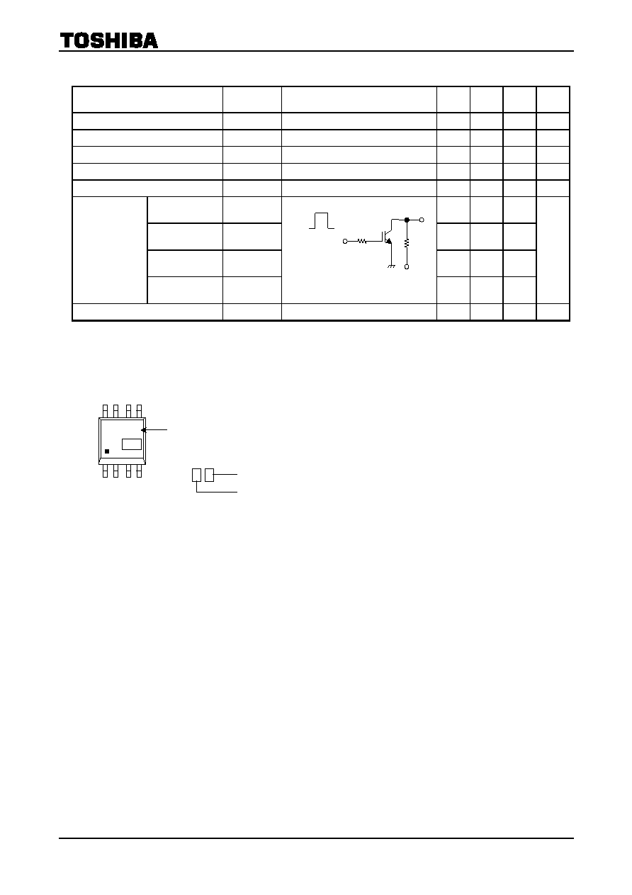
Unit: mm
JEDEC
JEITA
TOSHIBA 2-6J1C
Weight: 0.080 g (typ.)
Equivalent Circuit
1
2
3 4
5
7
8 6
GT8G132
2002-05-17
2
Electrical Characteristics
(Ta
=
=
=
=
25∞C)
Characteristics Symbol Test
Condition Min
Typ.
Max
Unit
Gate leakage current
I
GES
V
GE
=
±
6 V, V
CE
=
0
±
10
µ
A
Collector cut-off current
I
CES
V
CE
=
400 V, V
GE
=
0
10
µ
A
Gate-emitter cut-off voltage
V
GE (OFF)
I
C
=
1 mA, V
CE
=
5 V
0.6
1.2 V
Collector-emitter saturation voltage
V
CE (sat)
I
C
=
150 A, V
GE
=
4 V
2.3 7.0 V
Input capacitance
C
ies
V
CE
=
10 V, V
GE
=
0, f
=
1 MHz
2800
pF
Rise time
t
r
1.0
Turn-on time
t
on
1.1
Fall time
t
f
1.6
Switching time
Turn-off time
t
off
2.2
µ
s
Thermal resistance
(Note 2)
R
th (j-a)
114
∞C/W
Note 2: Drive operation: Mount on glass epoxy board [1 inch
2
◊
1.5 t]
Marking
V
IN
: t
r
<
=
100 ns
t
f
<
=
100 ns
Duty cycle
<
=
1%
4 V
0
51
300 V
2.
0
GT8G132
Type
Lot Number
Month (Starting from Alphabet A)
Year (Last Number of the Christian Era)

GT8G132
2002-05-17
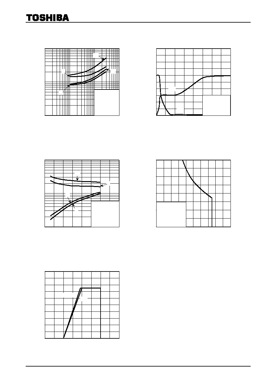
3
Co
lle
ct
o
r
cu
r
r
e
n
t
I C
(A
)
Co
lle
ct
o
r
cu
r
r
e
n
t
I C
(A
)
Collector-emitter voltage VCE (V)
Co
lle
ct
o
r
cu
r
r
e
n
t
I C
(A
)
Collector-emitter voltage VCE (V)
I
C
≠ V
CE
Co
lle
ct
o
r
cu
r
r
e
n
t
I C
(A
)
Collector-emitter voltage VCE (V)
I
C
≠ V
CE
Co
lle
ct
o
r
cu
r
r
e
n
t
I C
(A
)
Collector-emitter voltage VCE (V)
I
C
≠ V
CE
Gate-emitter voltage V
GE
(V)
I
C
≠ V
GE
Case temperature Tc (∞C)
V
CE (sat)
≠ Tc
C
o
l
l
e
ct
or
-em
i
tte
r s
a
tu
rati
on
vol
t
age
V
CE (sat)
(V
)
I
C
≠ V
CE
5
200
160
120
80
40
0
0 1 2 3 4
VGE
=
2.5 V
Common emitter
Tc
=
-
40∞C
3.5
3.0
5.0
4.5
4.0
5
200
160
120
80
40
0
0 1 2 3 4
Common emitter
Tc
=
25∞C
4.0
4.5
5.0
VGE
=
2.5 V
3.5
3.0
5
200
160
120
80
40
0
0 1 2 3 4
VGE
=
2.5 V
Common emitter
Tc
=
125∞C
4.0
5.0
4.5
3.5
3.0
5
200
160
120
80
40
0
0 1 2 3 4
Common emitter
Tc
=
70∞C
4.5
4.0
5.0
VGE
=
2.5 V
3.0
3.5
5
200
160
120
80
40
0
0 1 2 3 4
Tc
=
40∞C
Common emitter
VCE
=
5 V
25
70
125
160
3
2.5
1.5
1
0.5
0
-
80
-
40 0 40 80
120
2
Common emitter
VGE
=
4 V
IC
=
150 A
120
90
60

GT8G132
2002-05-17
4
Gate
-em
i
tt
er
cut
-
of
f
vol
t
ag
e V
GE (O
FF
)
(V
)
Co
lle
ct
o
r
-
e
m
i
tte
r
v
o
lta
g
e
V
CE
(
V
)
Gate-emitter voltage VGE (V)
Co
lle
ct
o
r
-
e
m
i
tte
r
v
o
lta
g
e
V
CE
(
V
)
Gate-emitter voltage VGE (V)
V
CE
≠ V
GE
Co
lle
ct
o
r
-
e
m
i
tte
r
v
o
lta
g
e
V
CE
(
V
)
Gate-emitter voltage VGE (V)
V
CE
≠ V
GE
Co
lle
ct
o
r
-
e
m
i
tte
r
v
o
lta
g
e
V
CE
(
V
)
Gate-emitter voltage VGE (V)
V
CE
≠ V
GE
Case temperature Tc (∞C)
V
GE (OFF)
≠ Tc
Collector-emitter voltage VCE (V)
C ≠ V
CE
C
apa
ci
ta
nce
C
(
p
F)
V
CE
≠ V
GE
5
4
3
2
1
0
5
0 1 2 3 4
IC
=
150 A
Common emitter
Tc
=
70∞C
120
90
60
5
5
4
3
2
1
0
0 1 2 3 4
IC
=
150 A
120
90
Common emitter
Tc
=
125∞C
60
5
5
4
3
2
1
0
0 1 2 3 4
Common emitter
Tc
=
-
40∞C
90
IC
=
150 A
120
60
5
5
4
3
2
1
0
0 1 2 3 4
Common emitter
Tc
=
25∞C
90
IC
=
150 A
120
60
1.4
1.2
0.8
0.4
0
-
80
-
40 0 40 80
160
Common emitter
VCE
=
5 V
IC
=
1 mA
1
0.6
0.2
120
10000
1000
100
1
10
1000
10 100
Common emitter
VGE
=
0 V
f
=
1 MHz
Tc
=
25∞C
Cies
Coes
Cres
GT8G132
2002-05-17
5
P
eak
col
l
e
ct
or
cu
rre
nt
I CP
(A
)
Mai
n
ca
paci
t
anc
e C
M
(
µ
F)
Switching Time ≠ R
G
Sw
itc
h
in
g
tim
e
(
µ
s)
Gate
-em
i
tt
er
volt
age
V
GE
(V
)
Gate charge QG (nC)
V
CE
, V
GE
≠ Q
G
Co
lle
ct
o
r
-
e
m
i
tte
r
v
o
lta
g
e
V
CE
(
V
)
Switching Time ≠ I
CP
Sw
itc
h
in
g
tim
e
(
µ
s)
Peak collector current ICP (A)
Maximum Operating Area
Minimum Gate Drive Area
Gate resistance RG (
)
Collector current IC (A)
Gate-emitter voltage VGE (V)
200
800
600
400
200
0
0 40 80 120
160
VCM
=
350 V
Tc
<=
70∞C
VGE
=
4.0 V
10
<=
RG
<
=
300
200
160
120
80
40
0
0 2 4 6 8
Tc
=
25∞C
70
1000
10
0.1
1 10
1
100
Common emitter
VCE
=
300 V
VGE
=
4 V
IC
=
150 A
Tc
=
25∞C
ton
toff
tf
tr
0
0
40 60 80
0
2
4
6
8
10
100
200
300
400
500
20
Common emitter
VCC
=
300 V
RL
=
2.0
Tc
=
25∞C
VCE
VGE
200
0 50 100
150
1
0.1
10
Common emitter
VCC
=
300 V
VGE
=
4 V
RG
=
51
Tc
=
25∞C
toff
tr
ton
tf

GT8G132
2002-05-17
6
∑
TOSHIBA is continually working to improve the quality and reliability of its products. Nevertheless, semiconductor
devices in general can malfunction or fail due to their inherent electrical sensitivity and vulnerability to physical
stress. It is the responsibility of the buyer, when utilizing TOSHIBA products, to comply with the standards of
safety in making a safe design for the entire system, and to avoid situations in which a malfunction or failure of
such TOSHIBA products could cause loss of human life, bodily injury or damage to property.
In developing your designs, please ensure that TOSHIBA products are used within specified operating ranges as
set forth in the most recent TOSHIBA products specifications. Also, please keep in mind the precautions and
conditions set forth in the "Handling Guide for Semiconductor Devices," or "TOSHIBA Semiconductor Reliability
Handbook" etc..
∑
The TOSHIBA products listed in this document are intended for usage in general electronics applications
(computer, personal equipment, office equipment, measuring equipment, industrial robotics, domestic appliances,
etc.). These TOSHIBA products are neither intended nor warranted for usage in equipment that requires
extraordinarily high quality and/or reliability or a malfunction or failure of which may cause loss of human life or
bodily injury ("Unintended Usage"). Unintended Usage include atomic energy control instruments, airplane or
spaceship instruments, transportation instruments, traffic signal instruments, combustion control instruments,
medical instruments, all types of safety devices, etc.. Unintended Usage of TOSHIBA products listed in this
document shall be made at the customer's own risk.
∑
The information contained herein is presented only as a guide for the applications of our products. No
responsibility is assumed by TOSHIBA CORPORATION for any infringements of intellectual property or other
rights of the third parties which may result from its use. No license is granted by implication or otherwise under
any intellectual property or other rights of TOSHIBA CORPORATION or others.
∑
The information contained herein is subject to change without notice.
000707EAA
RESTRICTIONS ON PRODUCT USE