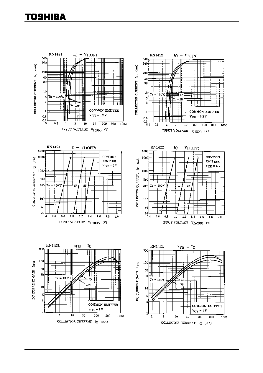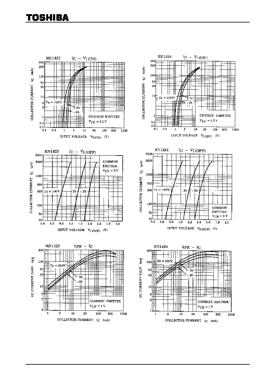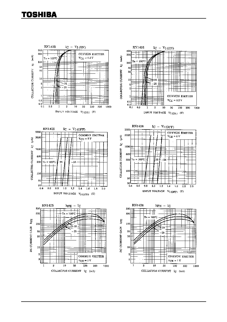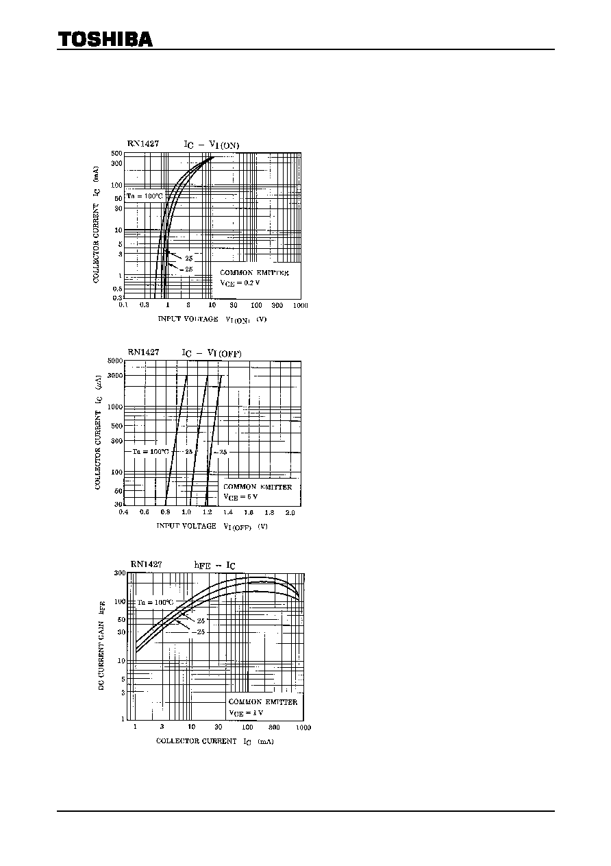
RN1421
~RN1427
2002-02-08
1
TOSHIBA Transistor Silicon NPN Epitaxial Type (PCT Process)
RN1421,RN1422,RN1423,RN1424
RN1425,RN1426,RN1427
Switching, Inverter Circuit, Interface Circuit
And Driver Circuit Applications
l High current type (I
C
(max) = 800mA)
l With built-in bias resistors
l Simplify circuit design
l Reduce a quantity of parts and manufacturing process
l Low V
CE
(sat)
l Complementary to RN2401~RN2406
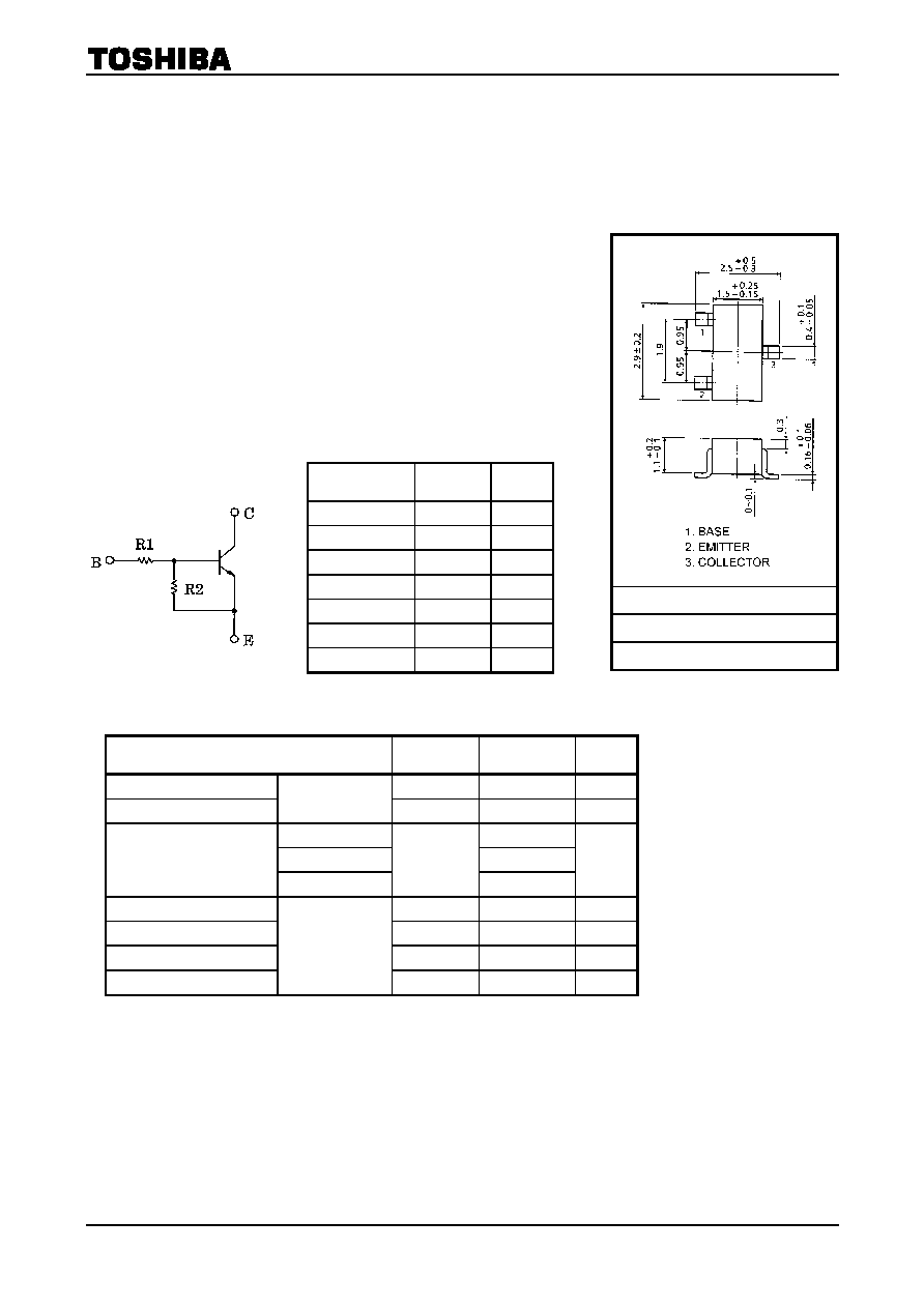
Equivalent Circuit and Bias Resister Values
Maximum Ratings
(Ta = 25°C)
Characteristic Symbol
Rating
Unit
Collector-base voltage
V
CBO
50 V
Collector-emitter voltage
RN1421~1427
V
CEO
50 V
RN1421~1424 10
RN1425, 1426
5
Emitter-base voltage
RN1427
V
EBO
6
V
Collector current
I
C
800
mA
Collector power dissipation
P
C
200
mW
Junction temperature
T
j
150
°C
Storage temperature range
RN1421~1427
T
stg
-55~150
°C
Unit: mm
JEDEC
JEITA SC-59
TOSHIBA 2-3F1A
Weight: 0.012 g (typ.)
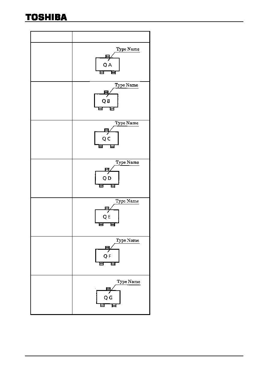
Type No.
R1 (k) R2
(k)
RN1421 1 1
RN1422 2.2
2.2
RN1423 4.7
4.7
RN1424 10 10
RN1425 0.47 10
RN1426 1 10
RN1427 2.2 10
RN1421
~RN1427
2002-02-08
2
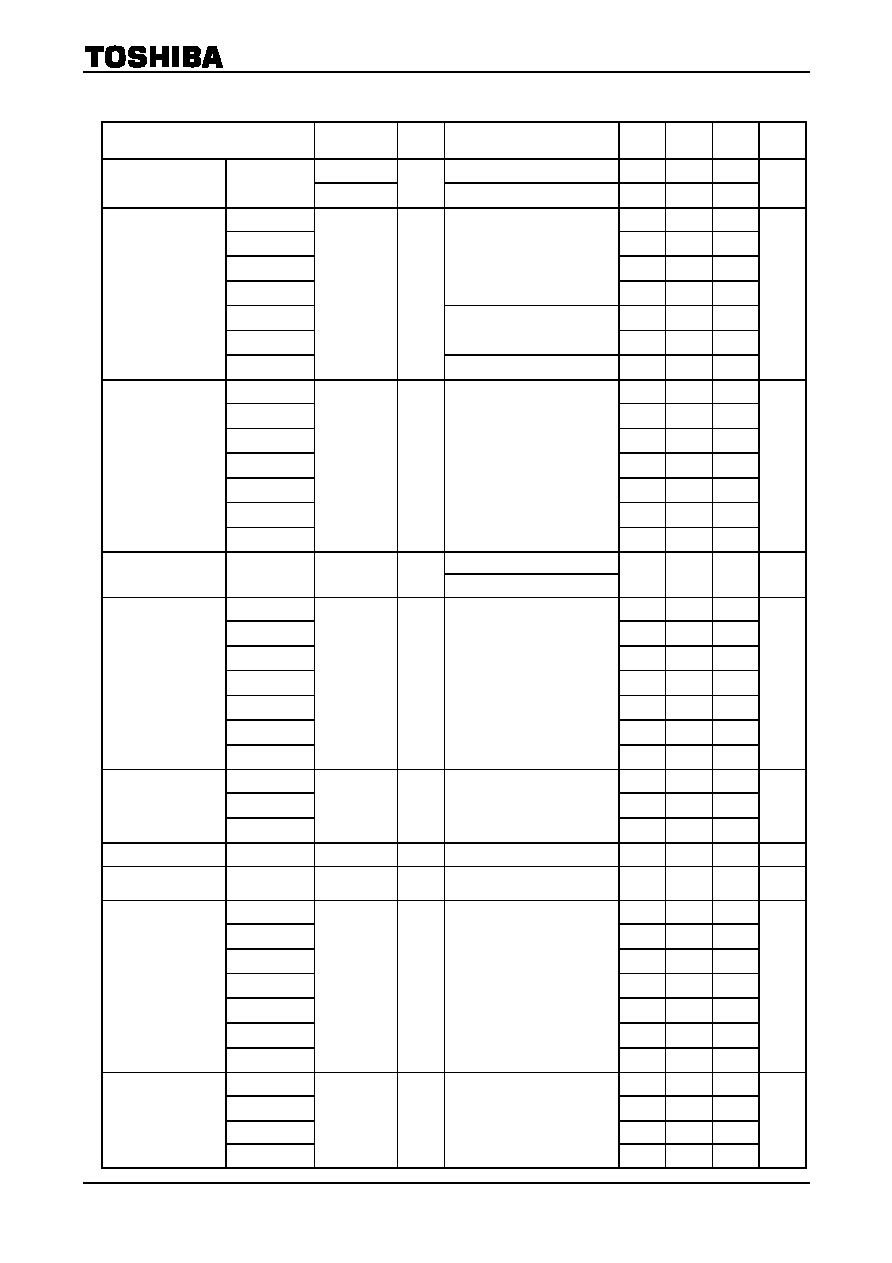
Electrical Characteristics (Ta = 25
°
C)
Characteristic Symbol
Test
Circuit
Test Condition
Min
Typ.
Max
Unit
I
CBO
V
CB
= 50V, I
E
= 0
100
Collector cut-off
current
RN1421~1427
I
CEO
V
CE
= 50V, I
B
= 0
500
nA
RN1421 3.85
7.14
RN1422 1.75
3.25
RN1423 0.82
1.52
RN1424
V
EB
= 10V, I
C
= 0
0.38
0.71
RN1425 0.365
0.682
RN1426
V
EB
= 5V, I
C
= 0
0.35
0.65
Emitter cut-off current
RN1427
I
EBO
V
EB
= 6V, I
C
= 0
0.378
0.703
mA
RN1421 60
RN1422 65
RN1423 70
RN1424 90
RN1425 90
RN1426 90
DC current gain
RN1427
h
FE
V
CE
= 1V, I
C
= 100mA
90
I
C
= 50mA, I
B
= 2mA
Collector-emitter
saturation voltage
RN1421~1427 V
CE (sat)
I
C
= 50mA, I
B
= 1mA
0.25
V
RN1421
1.0
3.5
RN1422
1.4
4.5
RN1423
2.0
6.5
RN1424
3.0
12.0
RN1425
0.6
2.0
RN1426
0.7
2.5
Input voltage (ON)
RN1427
V
I (ON)
V
CE
= 0.2V, I
C
= 100mA
1.0
3.0
V
RN1421~1424
0.8
1.3
RN1425, 1426
0.4
0.8
Input voltage (OFF)
RN1427
V
I (OFF)
V
CE
= 5V, I
C
= 0.1mA
0.5
1.0
V
Transition frequency RN1421~1427
f
T
V
CE
= 5V, I
C
= 20mA
300
MHz
Collector Output
capacitance
RN1421~1427 C
ob
V
CB
= 10V, I
E
= 0,
f = 1MH
z
7
pF
RN1421
0.7 1.0 1.3
RN1422
1.54 2.2 2.86
RN1423
3.29 4.7 6.11
RN1424
7 10 13
RN1425
0.329 0.47 0.61
RN1426
0.7 1.0 1.3
Input resistor
RN1427
R1
1.54 2.2 2.86
k
RN1421~1424
0.9 1.0 1.1
RN1425
0.0423 0.047 0.0517
RN1426
0.09 0.1 0.11
Resistor ratio
RN1427
R1/R2
0.2 0.22 0.24
RN1421
~RN1427
2002-02-08
8
· TOSHIBA is continually working to improve the quality and reliability of its products. Nevertheless, semiconductor
devices in general can malfunction or fail due to their inherent electrical sensitivity and vulnerability to physical
stress. It is the responsibility of the buyer, when utilizing TOSHIBA products, to comply with the standards of
safety in making a safe design for the entire system, and to avoid situations in which a malfunction or failure of
such TOSHIBA products could cause loss of human life, bodily injury or damage to property.
In developing your designs, please ensure that TOSHIBA products are used within specified operating ranges as
set forth in the most recent TOSHIBA products specifications. Also, please keep in mind the precautions and
conditions set forth in the "Handling Guide for Semiconductor Devices," or "TOSHIBA Semiconductor Reliability
Handbook" etc..
· The TOSHIBA products listed in this document are intended for usage in general electronics applications
(computer, personal equipment, office equipment, measuring equipment, industrial robotics, domestic appliances,
etc.). These TOSHIBA products are neither intended nor warranted for usage in equipment that requires
extraordinarily high quality and/or reliability or a malfunction or failure of which may cause loss of human life or
bodily injury ("Unintended Usage"). Unintended Usage include atomic energy control instruments, airplane or
spaceship instruments, transportation instruments, traffic signal instruments, combustion control instruments,
medical instruments, all types of safety devices, etc.. Unintended Usage of TOSHIBA products listed in this
document shall be made at the customer's own risk.
· The information contained herein is presented only as a guide for the applications of our products. No
responsibility is assumed by TOSHIBA CORPORATION for any infringements of intellectual property or other
rights of the third parties which may result from its use. No license is granted by implication or otherwise under
any intellectual property or other rights of TOSHIBA CORPORATION or others.
· The information contained herein is subject to change without notice.
000707EAA
RESTRICTIONS ON PRODUCT USE