 | –≠–ª–µ–∫—Ç—Ä–æ–Ω–Ω—ã–π –∫–æ–º–ø–æ–Ω–µ–Ω—Ç: T6K01 | –°–∫–∞—á–∞—Ç—å:  PDF PDF  ZIP ZIP |

T6K01
2002-01-07
1
TOSHIBA CMOS DIGITAL INTEGRATED CIRCUIT SILICON MONOLITHIC
T6K01
COLUMN DRIVER LSI FOR A DOT MATRIX GRAPHIC LCD
The T6K01 is a column (segment) driver for a dot matrix graphic
LCD. The T6K01 offers low power consumption, due to the CMOS
Si-Gate process. It is designed to interface directly with a
microprocessor unit (MPU). A program running on the MPU can
drive the T6K01 asynchronously. The T6K01 stores data
transferred from the MPU in its built-in RAM.
The data stored in the built-in display RAM corresponds to the
image on the LCD screen; the data is converted into the LCD
drive signal. A configuration of two T6K01s and one T6C03 can be
used to drive a 480 ◊ 160-dot LCD.
Features
l Dot matrix graphic LCD column driver with display RAM
l Display RAM capacity: 160 lines ◊ 240 outputs = 38400 bits
l LCD drive output: 240
l Interface: 8-bit MPU
l Relation between RAM data and display
RAM bit data = 1 display ON
RAM bit data = 0 display OFF
l Display OFF function
l Low power consumption
l Logic power supply: 2.7 to 3.3 V
l LCD power supply: 8.0 to 26.0 V
l CMOS Process
l Package: TCP (Tape Carrier Package)

T6K01
2002-01-07
2
Block Diagram

T6K01
2002-01-07
3
Pin Assignment
Note: The above diagram shows the pin configuration of the LSI chip; it does not show the configuration of the tape
carrier package.

T6K01
2002-01-07
4
Pin Functions
Pin Name
Pin No.
I / O
Functions
SEG1 to SEG240
46 to 285
Output
Column driver outputs
C
L
10 Input
Shift
clock
pulse
FP
11
Input
Display synchronous signal
FR 12
Input
Frame
signal
DB0 to DB7
13 to 20
I / O
Data bus
AD0 to AD12
21 to 33
Input
Address bus
R / W
34
Input
Read / write select
R / W = H Read selected
R / W = L Write selected
/ CE
35
Input
Chip enable
Data write: Data write enabled on rising edge of / CE
Data read: Data read out while / CE is at L level
/ DSPOF
36
Input
Display off. Usually connected to V
DD
.
/ DSPOF = H: Display-on mode. (SEG1 to SEG240) are operational.
/ DSPOF = L: Display-off mode. (SEG1 to SEG240) are at the V
SS
level.
/ RST
37
Input
Reset signal: / RST = L Reset state
DIR 38
Input
Data
direction
select
/ TEST1, 2
8, 9
Input
Test pin. Usually connected to V
DD
V
DD
, V
SS
7, 39
Power
supply
V
CCL
, V
CCR
V
LC0L
, V
LC0R
V
LC2L
, V
LC2R
V
LC3L
, V
LC3R
V
LC5L
, V
LC5R
HV
SSL
, HV
SSR
1, 45
2, 44
3, 43
4, 42
5, 41
6, 40
Power supply for LCD drive

T6K01
2002-01-07
5
Function of Each Block
RAM cell
The RAM capacity is 160 lines ◊ 240 outputs for a total of 38400 bits.
DIR
This circuit changes the data flow direction and page selection sequence.
Address decoder
This decoder selects one RAM address for read / write operation.
8-bit counter + decoder
The decoder selects one RAM cell from the 160 address lines for display operation.
Latch
The data is latched from the display RAM on the falling edge of C
L
.
Column driver circuit and LCD voltage generation circuit
The T6K01 has 240 column drivers and four different LCD drive output voltage levels. The display data
from the latch circuit and the M signal determine which of the four LCD drive voltages is selected. This
circuit is shown in the following diagram.
Relation Between FR, Data Input and Output Level
/ DSPOF
FR
Input Data (RAM Data)
Output Level
L
*
*
V
SS
/ V
LC5
H L
L
V
LC3
H L
H
V
SS
/ V
LC5
H H
L
V
LC2
H H
H
V
LC0
*: INVALID

T6K01
2002-01-07
6
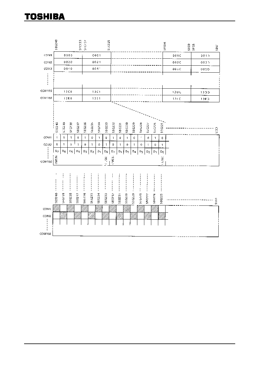
The relation between DIR and the memory map
(1) DIR = H
T6K01
2002-01-07
7
(2) DIR = L
T6K01
2002-01-07
8
Absolute Maximum Ratings
(Ta = 25∞C)
Item Symbol
Rating
Unit
Supply Voltage (1)
V
DD
(Note 2)
-0.3 to 6.5
V
Supply Voltage (2)
(Note 1, 2)
-0.3 to 28.0
V
Input Voltage
V
IN
(Note 2, 3)
-0.3 to V
DD
+0.3
V
Operating Temperature
T
opr
-20 to 75
∞C
Storage Temperature
T
stg
-55 to 125
∞C
Note 1: V
CCL
, V
CCR
, V
LC0L
, V
LC0R
, V
LC2L
, V
LC2R
, V
LC3L
, V
LC3R
, V
LC5L
and V
LC5R
Note 2: Referenced to V
SS
, HV
SSL
and HV
SSR
Note 3: Applies to all data bus and I / O pins.
Note 4: Ensure that the following condition is always maintained.
V
CCL
/ R
V
LC0L
/ R
VLC2L
/ R
VLC3L / R
V
LC5L / R
HV
SSL / R
T6K01
2002-01-07
9
Electrical Characteristics
DC Characteristics
Test Conditions
(Unless Otherwise Noted, V
SS
= 0 V, V
DD
= 3.0 V ± 10%, V
CCL / R
= 23.0 V ± 10%,
Ta = -20 to 75∞C)
Item Symbol
Test
Circuit
Test Condition
Min
Typ.
Max
Unit
Pin Name
Operating Supply (1)
V
DD
2.7
3.3 V
V
DD
Operating Supply (2)
V
CC
8.0
26.0 V V
CCL
, V
CCR
H Level
V
IH
0.7
V
DD
V
DD
V
Input
Voltage
L Level
V
IL
0
0.3
V
DD
V
DB0 to DB7
AD0 to AD7,
/
RST,
/
DSPOF,
/
CE, R
/
W,
D
/
I, C
L
, FP,
FR, DIR,
/
TEST
H Level
V
OH
I
OH
= -400 µA
V
DD
-0.4
V
DD
V
Output
Voltage
L Level
V
OL
I
OL
= 400 µA
V
SS
0.4 V
DB0 to DB7
Column Driver
Output Resistance
R
col
Load current = ±100 µA
(Note
4)
3.0 k
SEG1 to
SEG160
Input Leakage
I
IL
V
IN
= V
DD
to V
SS
-1
1 µA
DB0 to DB7
AD0 to AD7,
/
RST,
/
DSPOF,
/
CE, R
/
W,
D
/
I, C
L
, FP,
FR, DIR,
/
TEST
Operating Freq.
f
CL
10
50 kHz
C
L
Current Consumption
(1)
I
SS1
(Note
1)
410
520 µA
V
SS
, HV
SSL
,
HV
SSR
,
V
LC5L
, V
LC5R
Current Consumption
(2)
I
SS2
(Note
2)
45 65 µA
V
SS
, HV
SSL
,
HV
SSR
,
V
LC5L
, V
LC5R
Current Consumption
(3)
I
SS3
(Note
3)
-1
1 µA
V
SS
, HV
SSL
,
HV
SSR
,
V
LC5L
, V
LC5R
Note 1: Current consumption while internal data receiver is operating
V
DD
= 3.0 V ±10%, V
CCL
/ R = 23.0 V, Ta = 25∞C, 1 / 13 bias, 1 / 160 duty, no load, f
FP
= 70 Hz,
f
/ CE
= 5 MHz
Note 2: Current consumption while internal data receiver is sleeping
V
DD
= 3.0 V ±10%, V
CCL / R
= 23.0 V, Ta = 25∞C, 1 / 13 bias, 1 / 160 duty, no load, f
FP
= 70 Hz,
f
/ CE
= 0 Hz
Note 3: Standby current consumption
V
DD
= 3.0 V ±10%, V
CCL / R
= 23.0 V, Ta = 25∞C, no load, f
FP
= 0 Hz, f
/ CE
= 0 Hz
Note 4: V
CCL / R
= V
LC0L / R
= 23.0 V, V
LC2L / R
= V
CC
◊ 11 / 13, V
LC3L / R
= V
CC
◊ 2 / 13,
HV
SSL / R
= V
LC5L / R
= 0 V

T6K01
2002-01-07
10
AC Characteristics (1)
Test Conditions
(Unless Otherwise Noted, V
SS
= 0 V, V
DD
= 3.0 V ±10%, Ta = -20 to 75∞C)
Item Symbol
Min
Max
Unit
Enable Cycle Time
t
cycE
250
ns
Enable Pulse Width
PWEH
160
ns
Enable Rise / Fall Time
t
Er
, t
Ef
20 ns
Address Set-up Time
t
AS
0
ns
Address Hold Time
t
AH
10
ns
Data Set-up Time
t
DS
100
ns
Data Hold Time
t
DHW
20
ns
Data Delay Time
t
DD
(Note)
180
ns
Data Hold Time
t
DHR
(Note)
20
ns
Note: With load circuit connected
Load Circuit

T6K01
2002-01-07
11
AC Characteristics (2)
display data
Test Conditions
(Unless Otherwise Noted, V
SS
= 0 V, V
DD
= 3.0 V ± 10%, Ta = -20 to 75∞C)
Item Symbol
Pin
Name
Min
Max
Unit
C
L
Pulse Width H
t
CWH
C
L
500
ns
C
L
Pulse Width L
t
CWL
C
L
500
ns
C
L
Rise / Fall Time
t
r
, t
f
C
L
50 ns
FP Set-up Time
t
FSU
FP 100
ns
FP Hold Time
t
FHD
FP 100
ns
AC Characteristics
(3)
Item Symbol
Condition
Min
Max
Unit
C
L
-to-FP-margin time
t
CF
20
ns
FP-to-C
L
-margin time
t
FC
0
ns

T6K01
2002-01-07
12
Application Circuit

T6K01
2002-01-07
13
∑ TOSHIBA is continually working to improve the quality and reliability of its products. Nevertheless, semiconductor
devices in general can malfunction or fail due to their inherent electrical sensitivity and vulnerability to physical
stress. It is the responsibility of the buyer, when utilizing TOSHIBA products, to comply with the standards of
safety in making a safe design for the entire system, and to avoid situations in which a malfunction or failure of
such TOSHIBA products could cause loss of human life, bodily injury or damage to property.
In developing your designs, please ensure that TOSHIBA products are used within specified operating ranges as
set forth in the most recent TOSHIBA products specifications. Also, please keep in mind the precautions and
conditions set forth in the "Handling Guide for Semiconductor Devices," or "TOSHIBA Semiconductor Reliability
Handbook" etc..
∑ The TOSHIBA products listed in this document are intended for usage in general electronics applications
(computer, personal equipment, office equipment, measuring equipment, industrial robotics, domestic appliances,
etc.). These TOSHIBA products are neither intended nor warranted for usage in equipment that requires
extraordinarily high quality and/or reliability or a malfunction or failure of which may cause loss of human life or
bodily injury ("Unintended Usage"). Unintended Usage include atomic energy control instruments, airplane or
spaceship instruments, transportation instruments, traffic signal instruments, combustion control instruments,
medical instruments, all types of safety devices, etc.. Unintended Usage of TOSHIBA products listed in this
document shall be made at the customer's own risk.
∑ Polyimide base film is hard and thin. Be careful not to injure yourself on the film or to scratch any other parts with
the film. Try to design and manufacture products so that there is no chance of users touching the film after
assembly, or if they do , that there is no chance of them injuring themselves. When cutting out the film, try to
ensure that the film shavings do not cause accidents. After use, treat the leftover film and reel spacers as
industrial waste.
∑ Light striking a semiconductor device generates electromotive force due to photoelectric effects. In some cases
this can cause the device to malfunction.
This is especially true for devices in which the surface (back), or side of the chip is exposed. When designing
circuits, make sure that devices are protected against incident light from external sources. Exposure to light both
during regular operation and during inspection must be taken into account.
∑ The products described in this document are subject to the foreign exchange and foreign trade laws.
∑ The information contained herein is presented only as a guide for the applications of our products. No
responsibility is assumed by TOSHIBA CORPORATION for any infringements of intellectual property or other
rights of the third parties which may result from its use. No license is granted by implication or otherwise under
any intellectual property or other rights of TOSHIBA CORPORATION or others.
∑ The information contained herein is subject to change without notice.
000707EBE
RESTRICTIONS ON PRODUCT USE