 | –≠–ª–µ–∫—Ç—Ä–æ–Ω–Ω—ã–π –∫–æ–º–ø–æ–Ω–µ–Ω—Ç: TA2136F | –°–∫–∞—á–∞—Ç—å:  PDF PDF  ZIP ZIP |

TA2136F/N
2002-02-12
1
TOSHIBA Bipolar Liner Integrated Circuit Silicon Monolithic
TA2136F,TA2136N
Sound Retrieval System; 3D
Sound IC
The device incorporated the SRS; Sound Retrieval System under
license from SRS Labs, Inc.
The TA2136F/TA2136N is the IC with the Sound Retrieval
System to make 3D sound. It supports both stereo and monaural
signal inputs. This allows TA2136F/TA2136N to be suitable for
various audio systems such as TVs, stereo equipments, radio
cassette recorders, video game machines, electronic organs, and
PC units.
Features
∑ Incorporates three mode selectors.
(1) Monaural mode (SRS 3D mono)
(2) Stereo mode (SRS 3D stereo)
(3) Bypass mode (bypass mode)
∑ Center and space controlling functions
∑ Wide operation supply voltage
: V
CC (ope
.
)
= 4.5 to
12 V (Ta = 25)
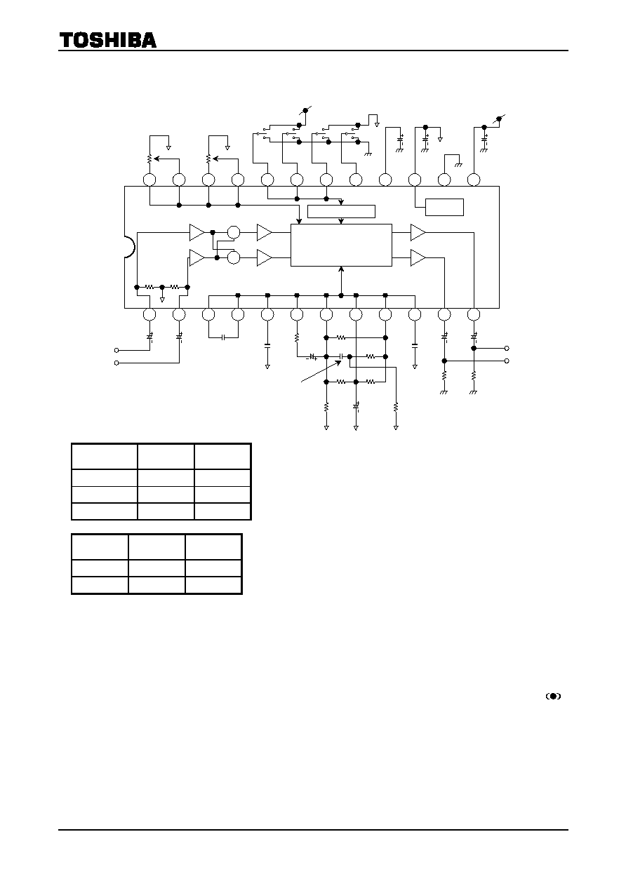
Block Diagram
Note 1: This device is vulnerable to surge voltages. Take it into account when using this device in your system.
The SRS; Sound Retrieval System and
are registered trademarks of SRS Labs, Inc.
TA2136F
TA2136N
Weight
SSOP24-P-300-1.00 : 0.31 g (typ.)
SDIP24-P-300-1.78 : 1.2 g (typ.)
R
-
L
L
+
R
SPO
U
T
+
-
8
9
7
5
6
4
3
2
1
12
11
10
17
16
18
20
19
21
22
23
24
13
14
15
Mode selector
Vref
3D FILTER
CT
I
N
CT
OUT
SP
IN
TES
T
MOD
E
1
MOD
E
2
MN
GN
V
CC
SMF
VR
EF
GND
BPF2
LI
N
RI
N
BPF1
PF3
BPF3
PF1
PF2
LOUT
PF4
PF5
ROUT
TA2136F/N
2002-02-12
2
Pin Function
Pin No.
Symbol
I/O
Function
Remarks
1
LIN
I
L channel signal input pin.
2
RIN
I
R channel signal input pin.
3 BPF1
æ
BPF1 pin for band pass filter.
4 BPF2
æ
BPF2 pin for band pass filter.
5 BPF3
æ
BPF3 pin for band pass filter.
6 PF1
æ
PF1 pin for 3D filter.
7 PF2
æ
PF2 pin for 3D filter.
8 PF3
æ
PF3 pin for 3D filter.
9 PF4
æ
PF4 pin for 3D filter.
10 PF5
æ
PF5 pin for 3D filter.
11
ROUT
O
R channel signal output pin.
12
LOUT
O
L channel signal output pin.
13 V
CC
æ
Power supply pin.
14 GND
æ
Ground
pin.
15 VREF
I
Reference
voltage
pin.
16 SMF
æ
SMF pin for smoothing filter.
17
TEST
I
Test pin, normally fixed "L" level.
18 MNGN
I
MNGN pin for monoral signal input gain selector.
Normally fixed "L" level.
19
MODE2
I
MODE2 pin for mode selector.
20
MODE1
I
MODE1 pin for mode selector.
21
SPOUT
O
Output pin for space control.
22
SPIN
I
Iutput pin for space control.
23
CTOUT
O
Output pin for center control.
24
CTIN
I
Input pin for center control.
TA2136F/N
2002-02-12
3
Application Circuit
Mode Mode1
Mode2
Bypass L
æ
3D mono
H
L
3D stereo
H
H
Level
Test
(Note 2)
MNGN
(Note 3)
L
-
3dB 0dB
H 0dB
-
6dB
Note 2: Usually, it is used by fixing to "L" level.
Note 3: Usually, it is not concerned with an L channel input or L and R channel input, but is used by fixing to "L"
level.
Note 4: The Sound Retrieval System (SRS) technology rights incorporated in the TA2136F/N are owned by SRS
Labs, a US Corporation and licensed to Toshiba Semiconductor. The Sound Retrieval System (SRS) is
protected under US and foreign patents used and/or pending. The Sound Retrieval System (SRS), the
and SRS symbol, are trademarks of SRS Labs, Inc. in the United States and selected foreign countries.
Neither the purchase of the TA2136F/N, nor the corresponding sale of audio enhancement equipment
conveys the right to sell commercialized recordings made with any SRS technology. SRS Labs requires that
all users of the TA2136F/N must enter into a license agreement directly with SRS Labs and comply with all
rules and regulations as outlined in the SRS Trademark Usage Manual.
R
-
L
L
+
R
100
m
F
V
CC
Vref
10
m
F
10
m
F
10 k
W
10 k
W
110 k
W
1.3 k
W
47 k
W
51 k
W
1 k
W
0.47
m
F
4700 pF
0.
01
m
F
4.
3 k
W
0.1
m
F
0.
1
m
F
0.
47
m
F
0.
47
m
F
0.
47
m
F
Lch-IN
Rch-IN
Lch-OUT
Rch-OUT
3.
9 k
W
+
-
51 k
W
51 k
W
Center
10 k
W
VR
Space
10 k
W
VR
8
9
7
5
6
4
3
2
1
12
11
10
17
16
18
20
19
21
22
23
24
13
14
15
MODE1 MODE2
TEST
MNGN
Mode selector
Vref
3D FILTER
10
m
F
4.
7
m
F

TA2136F/N
2002-02-12
4
Maximum Ratings
(Ta
=
=
=
=
25∞C)
Characteristics Symbol
Rating
Unit
Supply voltage
V
CC
12 V
TA2136F
(Note 5)
*
400
Power dissipation
P
d
TA2136N
(Note 6)
*
1200
mW
Operating temperature
T
opr
-
40 to 85
∞C
Storage temperature
T
stg
-
55 to 150
∞C
Note 5: Derated above 25∞C in the proportion of 3.2 mW/∞C
Note 6: Derated above 25∞C in the proportion of 9.6 mW/∞C
Electrical Characteristics
(unless otherwise specified, V
CC
=
=
=
=
9 V, f
=
=
=
=
1 kHz, RL
=
=
=
=
10 k
W
W
W
W
, V
in
=
=
=
=
-
-
-
-
10dBV, Rg
=
=
=
=
600
W
W
W
W
,
bypass mode, Ta
=
=
=
=
25∞C)
Characteristics Symbol
Test
Circuit
Test Condition
Min
Typ.
Max
Unit
Supply voltage
V
CC
æ
V
in
=
0
4.5
9
12
V
Iccq (BYP)
æ
V
in
=
0
æ
4 7
Iccq (SRS)
æ
V
in
=
0, SRS STEREO
æ
8 14
Supply current
Iccq (MONO)
æ
V
in
=
0, SRS MONO
æ
8 14
mA
Input resistance
Rin
æ
æ
40 50 60 k
W
Output clipping voltage
V
OCL
æ
THD
=
1%
1.4
1.7
æ
Vrms
THD (SRS)
æ
SRS STEREO,
Space&Center: max
æ
0.15
æ
THD (MONO)
æ
SRS
MONO
æ
0.2
æ
Total harmonic distortion
THD (BYP)
æ
SRS
BYPASS,
TEST
=
"H"
æ
0.004
æ
%
Bypass gain
V
(BYP)
æ
æ
-
5
-
3
-
1 dB
Output noise voltage
V
ON
(SRS)
æ
Input
=
GND,
Space&Center: MID
BW
=
20 Hz to 20 kHz
æ
35 50
m
Vrms
V
CH
æ
High
level
2
æ
V
CC
Mode select control voltage
V
CL
æ
Low
level
GND
æ
1
V
<Mode Select>
Mode Mode1 Mode2
Bypass L
æ
3D stereo
H
H
3D mono
H
L

TA2136F/N
2002-02-12
5
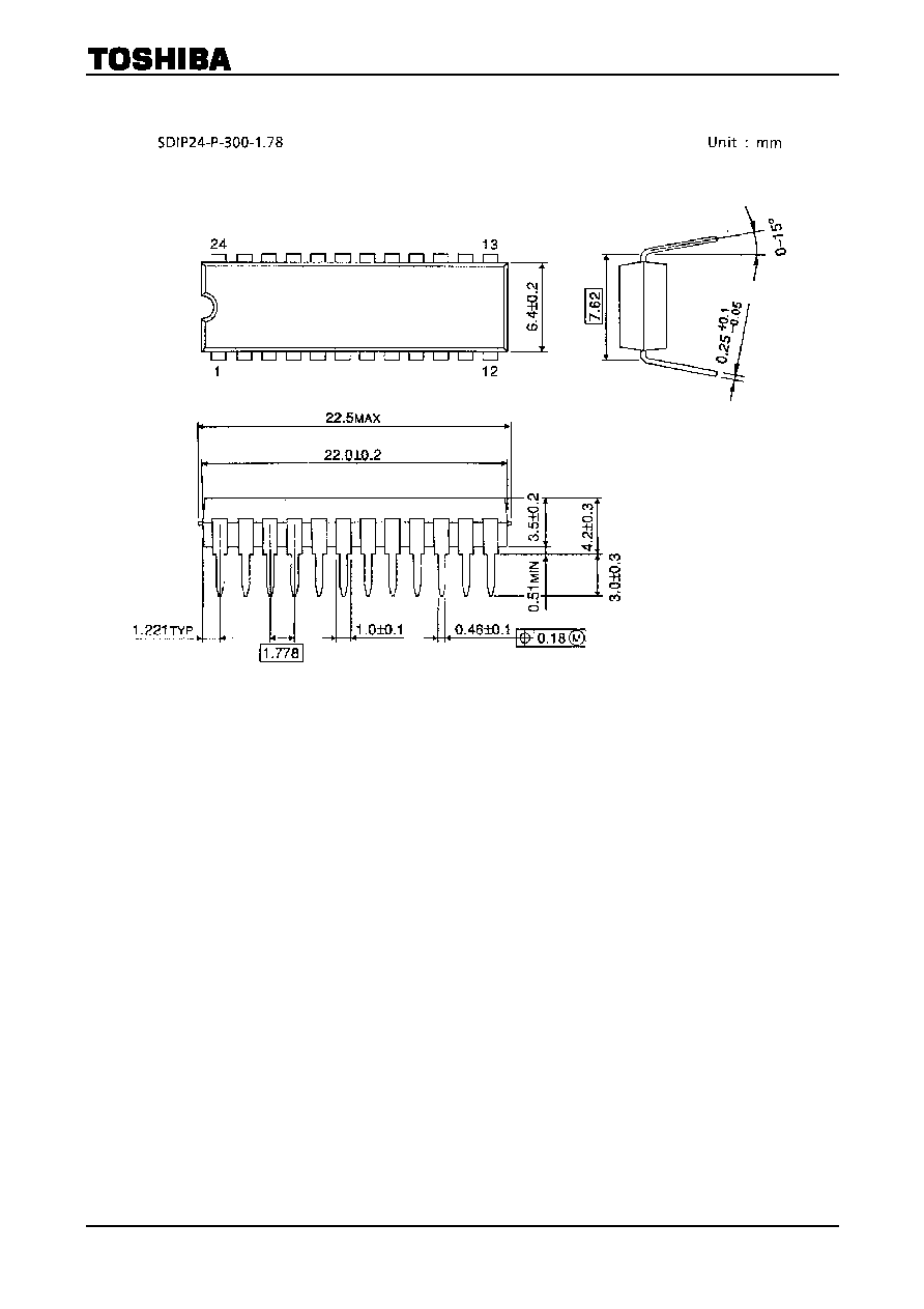
Package Dimensions
Weight: 0.31 g (typ.)
TA2136F/N
2002-02-12
6
Package Dimensions
Weight: 1.2 g (typ.)
TA2136F/N
2002-02-12
7
∑
TOSHIBA is continually working to improve the quality and reliability of its products. Nevertheless, semiconductor
devices in general can malfunction or fail due to their inherent electrical sensitivity and vulnerability to physical
stress. It is the responsibility of the buyer, when utilizing TOSHIBA products, to comply with the standards of
safety in making a safe design for the entire system, and to avoid situations in which a malfunction or failure of
such TOSHIBA products could cause loss of human life, bodily injury or damage to property.
In developing your designs, please ensure that TOSHIBA products are used within specified operating ranges as
set forth in the most recent TOSHIBA products specifications. Also, please keep in mind the precautions and
conditions set forth in the "Handling Guide for Semiconductor Devices," or "TOSHIBA Semiconductor Reliability
Handbook" etc..
∑
The TOSHIBA products listed in this document are intended for usage in general electronics applications
(computer, personal equipment, office equipment, measuring equipment, industrial robotics, domestic appliances,
etc.). These TOSHIBA products are neither intended nor warranted for usage in equipment that requires
extraordinarily high quality and/or reliability or a malfunction or failure of which may cause loss of human life or
bodily injury ("Unintended Usage"). Unintended Usage include atomic energy control instruments, airplane or
spaceship instruments, transportation instruments, traffic signal instruments, combustion control instruments,
medical instruments, all types of safety devices, etc.. Unintended Usage of TOSHIBA products listed in this
document shall be made at the customer's own risk.
∑
The products described in this document are subject to the foreign exchange and foreign trade laws.
∑
The information contained herein is presented only as a guide for the applications of our products. No
responsibility is assumed by TOSHIBA CORPORATION for any infringements of intellectual property or other
rights of the third parties which may result from its use. No license is granted by implication or otherwise under
any intellectual property or other rights of TOSHIBA CORPORATION or others.
∑
The information contained herein is subject to change without notice.
000707EBA
RESTRICTIONS ON PRODUCT USE