
TA78DL05,06,08,09,10,12,15AS
2003-01-29
1
TOSHIBA Bipolar Linear Integrated Circuit Silicon Monolithic
TA78DL05AS,TA78DL06AS,TA78DL08AS,TA78DL09AS,
TA78DL10AS,TA78DL12AS,TA78DL15AS
5 V, 6 V, 8 V, 9 V, 10 V, 12 V, 15 V
Three-Terminal Low Dropout Voltage Regulator
The TA78DL◊◊AS series consists of positive fixed output voltage
regulator IC capable of sourcing current up to 250 mA.
Due to the features of low dropout voltage and low standby
current, these devices are useful for battery powered equipment.
This series includes current limiting, thermal shutdown,
overvoltage protection, input fault protection and excessive
transient protection circuits internally.
Features
l Low standby current of 500 µA typical.
l Maximum output current up to 250 mA.
l Low dropout voltage of less than 0.6 V (@ I
OUT
= 0.2 A).
l Multi-protection:
Reverse connection of power supply, 60 V load dump, thermal shut down and current limiting.
l Metal fin (tab) is fully covered with mold resin. (TO-220 NIS package)
Pin Assignment
IN
1
3
OUT
GND
Marking side
2
Block Diagram
Weight: 1.7 g (typ.)
TA78DL05,06,08,09,10,12,15AS
2003-01-29
2
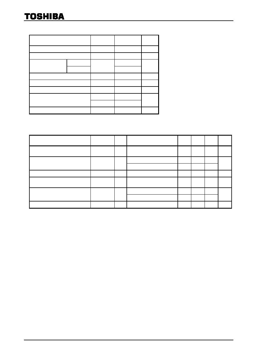
Maximum Ratings
(Ta = 25∞C)
Characteristics Symbol
Rating
Unit
Operating input voltage
V
IN
29 V
Input voltage of surge
V
IN
60 V
(Ta = 25∞C)
2
Power dissipation
(Tc = 25∞C)
P
D
20
W
Operating temperature
T
opr
-40~85 ∞C
Storage temperature
T
stg
-55~150 ∞C
Junction temperature
T
j
150 ∞C
R
th (j-c)
6.25
Thermal resistance
R
th (j-a)
62.5
∞C/W
Storage temperature∑time
T
sol
260
(10s)
∞C
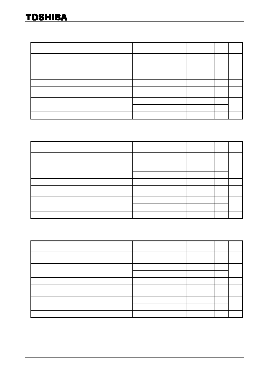
TA78DL05AS
Electrical Characteristics
(Unless otherwise specified, V
IN
= 14 V, I
OUT
= 10 mA, T
j
= 25∞C)
Characteristics Symbol
Test
Circuit
Test Condition
Min
Typ.
Max
Unit
Output voltage
V
OUT
5.35 V V
IN
26 V,
-40∞C Ta 85∞C
4.75 5.0 5.25
V
9 V V
IN
16 V
2 10
Line regulation
Reg∑line
6 V V
IN
26 V
4 30
mV
Load regulation
Reg∑load
10
mA
I
OUT
200 mA
14 50 mV
Quiescent current
I
B
I
OUT
10 mA,
6 V V
IN
26 V
0.5 1 mA
I
OUT
= 50 mA
0.15 0.3
Dropout voltage
V
D
I
OUT
= 200 mA
0.4 0.6
V
Max operating voltage
V
IN
29
33
V
TA78DL05,06,08,09,10,12,15AS
2003-01-29
3
TA78DL06AS
Electrical Characteristics
(Unless otherwise specified, V
IN
= 14 V, I
OUT
= 10 mA, T
j
= 25∞C)
Characteristics Symbol
Test
Circuit
Test Condition
Min
Typ.
Max
Unit
Output voltage
V
OUT
6.35 V V
IN
26 V,
-40∞C Ta 85∞C
5.7 6.0 6.3 V
10 V V
IN
17 V
2 12
Line regulation
Reg∑line
7 V V
IN
26 V
5 36
mV
Load regulation
Reg∑load
10
mA
I
OUT
200 mA
17 60 mV
Quiescent current
I
B
I
OUT
10 mA,
7 V V
IN
26 V
0.55 mA
I
OUT
= 50 mA
0.15 0.3
Dropout voltage
V
D
I
OUT
= 200 mA
0.4 0.6
V
Max operating voltage
V
IN
29
33
V
TA78DL08AS
Electrical Characteristics
(Unless otherwise specified, V
IN
= 16 V, I
OUT
= 10 mA, T
j
= 25∞C)
Characteristics Symbol
Test
Circuit
Test Condition
Min
Typ.
Max
Unit
Output voltage
V
OUT
8.35 V V
IN
26 V,
-40∞C Ta 85∞C
7.6 8 8.4 V
12 V V
IN
19 V
3 16
Line regulation
Reg∑line
9 V V
IN
26 V
6 45
mV
Load regulation
Reg∑load
10
mA
I
OUT
200 mA
22 80 mV
Quiescent current
I
B
I
OUT
10 mA,
9 V V
IN
26 V
0.6 mA
I
OUT
= 50 mA
0.15 0.3
Dropout voltage
V
D
I
OUT
= 200 mA
0.4 0.6
V
Max operating voltage
V
IN
29
33
V
TA78DL09AS
Electrical Characteristics
(Unless otherwise specified, V
IN
= 16 V, I
OUT
= 10 mA, T
j
= 25∞C)
Characteristics Symbol
Test
Circuit
Test Condition
Min
Typ.
Max
Unit
Output voltage
V
OUT
9.35 V V
IN
26 V,
-40∞C Ta 85∞C
8.55 9 9.45
V
13 V V
IN
20 V
3 18
Line regulation
Reg∑line
10 V V
IN
26 V
7 50
mV
Load regulation
Reg∑load
10
mA
I
OUT
200 mA
25 90 mV
Quiescent current
I
B
I
OUT
10 mA,
10 V V
IN
26 V
0.65 mA
I
OUT
= 50 mA
0.15 0.3
Dropout voltage
V
D
I
OUT
= 200 mA
0.4 0.6
V
Max operating voltage
V
IN
29
33
V

TA78DL05,06,08,09,10,12,15AS
2003-01-29
4
TA78DL10AS
Electrical Characteristics
(Unless otherwise specified, V
IN
= 16 V, I
OUT
= 10 mA, T
j
= 25∞C)
Characteristics Symbol
Test
Circuit
Test Condition
Min
Typ.
Max
Unit
Output voltage
V
OUT
10.35 V V
IN
26 V,
-40∞C Ta 85∞C
9.5 10 10.5
V
14 V V
IN
21 V
4 20
Line regulation
Reg∑line
11 V V
IN
26 V
8 60
mV
Load regulation
Reg∑load
10
mA
I
OUT
200 mA
28 100
mV
Quiescent current
I
B
I
OUT
10 mA,
11 V V
IN
26 V
0.7 mA
I
OUT
= 50 mA
0.15 0.3
Dropout voltage
V
D
I
OUT
= 200 mA
0.4 0.6
V
Max operating voltage
V
IN
29
33
V
TA78DL12AS
Electrical Characteristics
(Unless otherwise specified, V
IN
= 18 V, I
OUT
= 10 mA, T
j
= 25∞C)
Characteristics Symbol
Test
Circuit
Test Condition
Min
Typ.
Max
Unit
Output voltage
V
OUT
12.35 V V
IN
26 V,
-40∞C Ta 85∞C
11.4 12 12.6
V
16 V V
IN
23 V
5 24
Line regulation
Reg∑line
13 V V
IN
26 V
10 70
mV
Load regulation
Reg∑load
10
mA
I
OUT
200 mA
33 120
mV
Quiescent current
I
B
I
OUT
10 mA,
13 V V
IN
26 V
0.8 mA
I
OUT
= 50 mA
0.15 0.3
Dropout voltage
V
D
I
OUT
= 200 mA
0.4 0.6
V
Max operating voltage
V
IN
29
33
V
TA78DL15AS
Electrical Characteristics
(Unless otherwise specified, V
IN
= 20 V, I
OUT
= 10 mA, T
j
= 25∞C)
Characteristics Symbol
Test
Circuit
Test Condition
Min
Typ.
Max
Unit
Output voltage
V
OUT
15.35 V V
IN
26 V,
-40∞C Ta 85∞C
14.25 15 15.75
V
19 V V
IN
26 V
6 30
Line regulation
Reg∑line
16 V V
IN
26 V
12 80
mV
Load regulation
Reg∑load
10
mA
I
OUT
200 mA
40 150
mV
Quiescent current
I
B
I
OUT
10 mA,
16 V V
IN
26 V
0.9 mA
I
OUT
= 50 mA
0.15 0.3
Dropout voltage
V
D
I
OUT
= 200 mA
0.4 0.6
V
Max operating voltage
V
IN
29
33
V

TA78DL05,06,08,09,10,12,15AS
2003-01-29
5
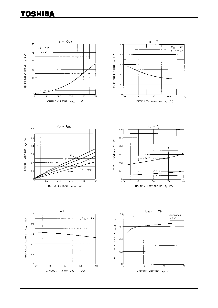
Application Circuit
Capacitor C
IN
/C
OUT
must be guaranteed to operate of the temperature range that the regulator should be operated
correctly.
The equivalent series resistance (ESR) of C
OUT
must be less than 1 in operating temperature range.

TA78DL05,06,08,09,10,12,15AS
2003-01-29
6
TA78DL05,06,08,09,10,12,15AS
2003-01-29
7

TA78DL05,06,08,09,10,12,15AS
2003-01-29
8
Package Dimensions
Weight: 1.7 g (typ.)

TA78DL05,06,08,09,10,12,15AS
2003-01-29
9
∑ TOSHIBA is continually working to improve the quality and reliability of its products. Nevertheless, semiconductor
devices in general can malfunction or fail due to their inherent electrical sensitivity and vulnerability to physical
stress. It is the responsibility of the buyer, when utilizing TOSHIBA products, to comply with the standards of
safety in making a safe design for the entire system, and to avoid situations in which a malfunction or failure of
such TOSHIBA products could cause loss of human life, bodily injury or damage to property.
In developing your designs, please ensure that TOSHIBA products are used within specified operating ranges as
set forth in the most recent TOSHIBA products specifications. Also, please keep in mind the precautions and
conditions set forth in the "Handling Guide for Semiconductor Devices," or "TOSHIBA Semiconductor Reliability
Handbook" etc..
∑ The TOSHIBA products listed in this document are intended for usage in general electronics applications
(computer, personal equipment, office equipment, measuring equipment, industrial robotics, domestic appliances,
etc.). These TOSHIBA products are neither intended nor warranted for usage in equipment that requires
extraordinarily high quality and/or reliability or a malfunction or failure of which may cause loss of human life or
bodily injury ("Unintended Usage"). Unintended Usage include atomic energy control instruments, airplane or
spaceship instruments, transportation instruments, traffic signal instruments, combustion control instruments,
medical instruments, all types of safety devices, etc.. Unintended Usage of TOSHIBA products listed in this
document shall be made at the customer's own risk.
∑ The products described in this document are subject to the foreign exchange and foreign trade laws.
∑ The information contained herein is presented only as a guide for the applications of our products. No
responsibility is assumed by TOSHIBA CORPORATION for any infringements of intellectual property or other
rights of the third parties which may result from its use. No license is granted by implication or otherwise under
any intellectual property or other rights of TOSHIBA CORPORATION or others.
∑ The information contained herein is subject to change without notice.
000707EBA
RESTRICTIONS ON PRODUCT USE