
TC74LCX652FS
2002-01-11
1
TOSHIBA CMOS Digital Integrated Circuit Silicon Monolithic
TC74LCX652FS
Low-Voltage Octal Bus Transceiver/Register with 5-V Tolerant Inputs and Outputs
The TC74LCX652FS is a high-performance CMOS octal bus
transceiver/register. Designed for use in 3.3-V systems, it
achieves high-speed operation while maintaining the CMOS low
power dissipation.
This device is designed for low-voltage (3.3 V) V
CC
applications,
but it could be used to interface to 5-V supply environment for
both inputs and outputs.
This device is bus transceiver with 3-state outputs, D-type
flip-flops, and control circuitry arranged for multiplexed
transmission of data directly from the internal registers.
All inputs are equipped with protection circuits against static
discharge.
Features
∑ Low-voltage operation: V
CC
= 2.0 to 3.6 V
∑ High-speed operation: t
pd
= 7.0 ns (max) (V
CC
= 3.0 to 3.6 V)
∑ Output current: |I
OH
|/I
OL
= 24 mA (min) (V
CC
= 3.0 V)
∑ Latch-up performance: ±500 mA
∑ Available in SSOP
∑ Bidirectional interface between 5 V and 3.3 V signals
∑ Power-down protection provided on all inputs and outputs
∑ Pin and function compatible with the 74 series (74AC/F/ALS/LS etc.) 652 type
Note 1: Do not apply a signal to any bus pins when it is in the output mode. Damage may result.
All floating (high impedance) bus pins must have their input levels fixed by means of pull-up or pull-down
resistors.
Weight: 0.14 g (typ.)

TC74LCX652FS
2002-01-11
2
Pin Assignment
(top view)
IEC Logic Symbol
21
3
23
22
1
2
EN1 [BA]
EN2 [AB]
C4
G5
C6
G7
OEBA
OEAB
CBA
SBA
CAB
SAB
>
1
1
5 4D
5
1
6D 7
1
7
>
1
2
B1
B2
B3
B4
B5
B6
B7
B8
19
18
17
16
15
14
13
20
4
5
6
7
8
9
10
11
A1
A2
A3
A4
A5
A6
A7
A8
V
CC
24
CBA
SBA
OEBA
B1
B2
23
22
21
20
19
18
CAB
1
2
3
4
5
6
7
SAB
OEAB
A1
A2
A3
A4
B3
8
A5
17 B4
9
10
11
12
16
15
14
A8
GND
A7
A6
B8
B7
B6
B5
13
TC74LCX652FS
2002-01-11
3
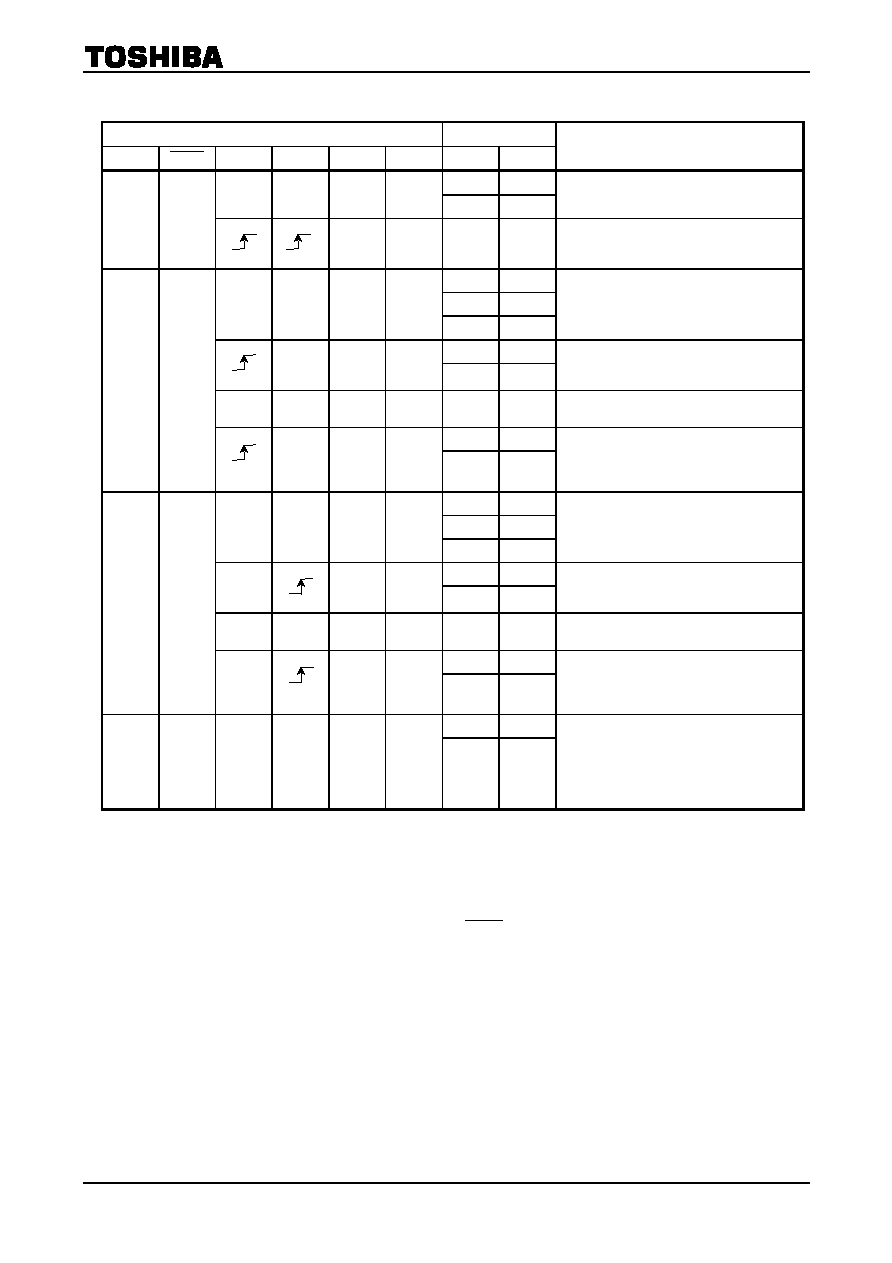
Truth Table
Control Inputs
Bus
OEAB
OEBA
CAB CBA SAB SBA
A
B
Function
Input Input
X
*
X
*
X X
Z Z
The output functions of A and B busses are
disabled.
L H
X X X X
Both A and B busses are used as inputs to
the internal flip-flops. Data on the bus will be
stored on the rising edge of the Clock.
Input Output
L L
X
*
X
*
L X
H H
The data on the A bus are displayed on the
B bus.
L L
X
*
L X
H H
The data on the A bus are displayed on the
B bus, and are stored into the A storage
flip-flops on the rising edge of CAB.
X
*
X
*
H X X Qn
The data in the A storage flop-flops are
displayed on the B bus.
L L
H H
X
*
H X
H H
The data on the A bus are stored into the A
storage flip-flops on the rising edge of CAB,
and the stored data propagate directly onto
the B bus.
Output
Input
L L
X
*
X
*
X L
H H
The data on the B bus are displayed on the
A bus.
L L
X
*
X L
H H
The data on the B bus are displayed on the
A bus, and are stored into the B storage
flip-flops on the rising edge of CBA.
X
*
X
*
X H Qn X
The data in the B storage flip-flops are
displayed on the A bus.
L L
L L
X
*
X H
H H
The data on the B bus are stored into the B
storage flip-flops on the rising edge of CBA,
and the stored data propagate directly onto
the A bus.
Output
Output
H L X
*
X
*
H H
Qn Qn
The data in the A storage flop-flops are
displayed on the B bus, and the data in the B
storage flop-flops are displayed on the A.
X: Don't care
Z: High impedance
Q
n
: The data stored into the internal flip-flops by most recent low to high transition of the clock inputs.
*
: The clocks are not internally gated with either OEAB or OEBA .
Therefore, data on the A and/or B busses may be clocked into the storage flip-flops at any time.

TC74LCX652FS
2002-01-11
4
System Diagram
Timing Chart
A: Input
B: Output
A: Output
B: Input
OEAB
OEBA
SAB
SBA
CAB
CBA
A
B
: Don't care
D Q
CK
Q D
CK
B8
CBA
SBA
B1
20
13
23
22
11
1
2
A8
CAB
SAB
OEAB
OEBA
A1
3
21
4
Same as above block
f
A
f
B
f
B
f
A
A
B
A
B
B
B
B
B

TC74LCX652FS
2002-01-11
5
Maximum Ratings
Characteristics Symbol Rating Unit
Power supply voltage
V
CC
-
0.5 to 7.0
V
DC input voltage
(CAB, CBA, SAB, SBA, OEAB,
OEBA
)
V
IN
-
0.5 to 7.0
V
-
0.5 to 7.0 (Note 2)
DC bus I/O voltage
V
I/O
-
0.5 to V
CC
+
0.5
(Note
3)
V
Input diode current
I
IK
-
50 mA
Output diode current
I
OK
±
50 (Note
4)
mA
DC output current
I
OUT
±
50 mA
Power dissipation
P
D
180 mW
DC V
CC
/ground current
I
CC
/I
GND
±
100 mA
Storage temperature
T
stg
-
65 to 150
∞C
Note 2: Output in OFF state
Note 3: High or low state. I
OUT
absolute maximum rating must be observed.
Note 4: V
OUT
<
GND, V
OUT
>
V
CC
Recommended Operating Conditions
Characteristics Symbol Rating Unit
2.0 to 3.6
Power supply voltage
V
CC
1.5 to 3.6 (Note 5)
V
Input voltage
(CAB, CBA, SAB, SBA, OEAB,
OEBA
)
V
IN
0 to 5.5
V
0 to 5.5
(Note 6)
Bus I/O voltage
V
I/O
0
to
V
CC
(Note
7)
V
±
24 (Note
8)
Output current
I
OH
/I
OL
±
12 (Note
9)
mA
Operating temperature
T
opr
-
40 to 85
∞C
Input rise and fall time
dt/dv
0 to 10 (Note 10)
ns/V
Note 5: Data retention only
Note 6: Output in OFF state
Note 7: High or low state
Note 8: V
CC
=
3.0 to 3.6 V
Note 9: V
CC
=
2.7 to 3.0 V
Note 10: V
IN
=
0.8 to 2.0 V, V
CC
=
3.0 V