
TC74LCX74F/FN/FT
2002-01-11
1
TOSHIBA CMOS Digital Integrated Circuit Silicon Monolithic
TC74LCX74F,TC74LCX74FN,TC74LCX74FT
Low-Voltage Dual D-Type Flip-Flop with 5-V Tolerant Inputs and Outputs
The TC74LCX74F/FN/FT is a high-performance CMOS D-type
flip-flop. Designed for use in 3.3-V systems, it achieves
high-speed operation while maintaining the CMOS low power
dissipation.
The device is designed for low-voltage (3.3 V) V
CC
applications,
but it could be used to interface to 5-V supply environment for
inputs.
The signal level applied to the D input is transferred to Q
output during the positive going transition of the CK pulse. CLR
and PR are independent of the CK and are accomplished by
setting the appropriate input low.
All inputs are equipped with protection circuits against static
discharge.
Features
∑ Low-voltage operation: V
CC
= 2.0 to 3.6 V
∑ High-speed operation: t
pd
= 7.0 ns (max) (V
CC
= 3.0 to 3.6 V)
∑ Output current: |I
OH
|/I
OL
= 24 mA (min) (V
CC
= 3.0 V)
∑ Latch-up performance: ±500 mA
∑ Available in JEDEC SOP, JEITA SOP and TSSOP
∑ Power-down protection provided on all inputs and outputs
∑ Pin and function compatible with the 74 series
(74AC/VHC/HC/F/ALS/LS etc.) 74 type
Note: xxxFN (JEDEC SOP) is not available in
Japan.
TC74LCX74F
TC74LCX74FN
TC74LCX74FT
Weight
SOP14-P-300-1.27: 0.18 g (typ.)
SOL14-P-150-1.27: 0.12 g (typ.)
TSSOP14-P-0044-0.65: 0.06 g (typ.)

TC74LCX74F/FN/FT
2002-01-11
2
Pin Assignment
(top view)
IEC Logic Symbol
Truth Table
Inputs Outputs
CLR
PR
D CK Q
Q
Function
L H X X L H
Clear
H L X X H L
Preset
L L X X H H
æ
H H L L H
æ
H H H H L
æ
H H X Qn
n
Q
No
change
X: Don't care
Maximum Ratings
Characteristics Symbol Rating
Unit
Power supply voltage
V
CC
-
0.5 to 7.0
V
DC input voltage
V
IN
-
0.5 to 7.0
V
-
0.5 to 7.0 (Note 1)
DC output voltage
V
OUT
-
0.5 to V
CC
+
0.5
(Note
2)
V
Input diode current
I
IK
-
50 mA
Output diode current
I
OK
±
50 (Note
3)
mA
DC output current
I
OUT
±
50 mA
Power dissipation
P
D
180 mW
DC V
CC
/ground current
I
CC
/I
GND
±
100 mA
Storage temperature
T
stg
-
65 to 150
∞C
Note 1: V
CC
=
0 V
Note 2: High or low state. I
OUT
absolute maximum rating must be observed.
Note 3: V
OUT
<
GND, V
OUT
>
V
CC
V
CC
CLR
2
2D
2CK
PR
2
2Q
14
13
12
11
10
CLR
1
1
2
3
4
5
6
7
1D
1CK
PR
1
1Q
Q
1
GND
Q
2
9
8
CK
Q
D
Q
CK
Q
D
Q
3
S
4
1
2
11
10
13
12
1CK
PR
1
1D
2CK
2D
5
6
9
8
1Q
Q
1
2Q
Q
2
PR
2
CLR
1
CLR
2
C1
1D
R

TC74LCX74F/FN/FT
2002-01-11
3
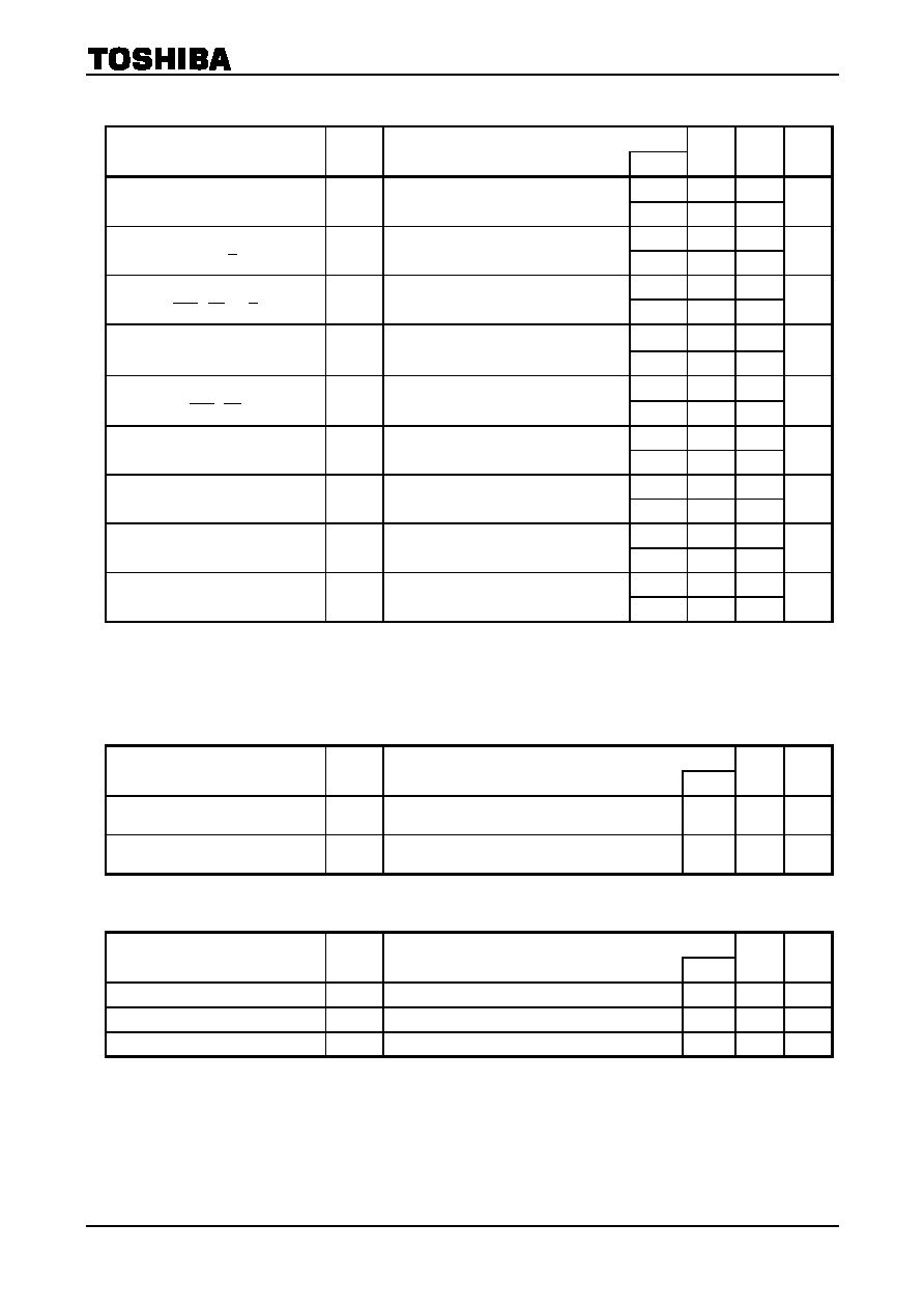
Recommended Operating Conditions
Characteristics Symbol Rating
Unit
2.0 to 3.6
Power supply voltage
V
CC
1.5 to 3.6 (Note 4)
V
Input voltage
V
IN
0 to 5.5
V
0 to 5.5 (Note 5)
Output voltage
V
OUT
0
to
V
CC
(Note 6)
V
±
24 (Note
7)
Output current
I
OH
/I
OL
±
12 (Note
8)
mA
Operating temperature
T
opr
-
40 to 85
∞C
Input rise and fall time
dt/dv
0 to 10 (Note 9)
ns/V
Note 4: Data retention only
Note 5: V
CC
=
0 V
Note 6: High or low state
Note 7: V
CC
=
3.0 to 3.6 V
Note 8: V
CC
=
2.7 to 3.0 V
Note 9: V
IN
=
0.8 to 2.0 V, V
CC
=
3.0 V
Electrical Characteristics
DC Characteristics
(Ta
=
=
=
=
-
-
-
-
40 to 85∞C)
Characteristics Symbol
Test
Condition
V
CC
(V)
Min Max
Unit
H-level
V
IH
æ
2.7 to 3.6
2.0
æ
Input voltage
L-level V
IL
æ
2.7 to 3.6
æ
0.8
V
I
OH
=
-
100
m
A
2.7 to 3.6 V
CC
-
0.2
æ
I
OH
=
-
12 mA
2.7
2.2
æ
I
OH
=
-
18 mA
3.0
2.4
æ
H-level
V
OH
V
IN
=
V
IH
or V
IL
I
OH
=
-
24 mA
3.0
2.2
æ
I
OL
=
100
m
A
2.7 to 3.6
æ
0.2
I
OL
=
12 mA
2.7
æ
0.4
I
OL
=
16 mA
3.0
æ
0.4
Output voltage
L-level V
OL
V
IN
=
V
IH
or V
IL
I
OL
=
24 mA
3.0
æ
0.55
V
Input leakage current
I
IN
V
IN
=
0 to 5.5 V
2.7 to 3.6
æ
±
5.0
m
A
Power-off leakage current
I
OFF
V
IN
/V
OUT
=
5.5 V
0
æ
10.0
m
A
V
IN
=
V
CC
or GND
2.7 to 3.6
æ
10.0
Quiescent supply current
I
CC
V
IN
=
3.6 to 5.5 V
2.7 to 3.6
æ
±
10.0
Increase in I
CC
per input
D
I
CC
V
IH
=
V
CC
-
0.6
V
2.7 to 3.6
æ
500
m
A
TC74LCX74F/FN/FT
2002-01-11
4
AC Characteristics
(Ta
=
=
=
=
-
-
-
-
40 to 85∞C)
Characteristics Symbol
Test
Condition
V
CC
(V)
Min Max
Unit
2.7
æ
æ
Maximum clock frequency
f
max
Figure 1, Figure 2
3.3
±
0.3
150
æ
MHz
2.7
æ
8.0
Propagation delay time
(CK-Q,
Q
)
t
pLH
t
pHL
Figure 1, Figure 2
3.3
±
0.3
1.5
7.0
ns
2.7
æ
8.0
Propagation delay time
(
CLR
,
PR
-Q,
Q
)
t
pLH
t
pHL
Figure 1, Figure 4
3.3
±
0.3
1.5
7.0
ns
2.7 3.3
æ
Minimum pulse width
(CK)
t
W
(H)
t
W
(L)
Figure 1, Figure 2
3.3
±
0.3
3.3
æ
ns
2.7 3.6
æ
Minimum pulse width
(
CLR
,
PR
)
t
W
(L) Figure 1, Figure 4
3.3
±
0.3
3.3
æ
ns
2.7 2.5
æ
Minimum setup time
t
s
Figure 1, Figure 2
3.3
±
0.3
2.5
æ
ns
2.7 1.5
æ
Minimum hold time
t
h
Figure 1, Figure 2
3.3
±
0.3
1.5
æ
ns
2.7 3.0
æ
Minimum removal time
t
rem
Figure 1, Figure 3
3.3
±
0.3
2.5
æ
ns
2.7
æ
æ
Output to output skew
t
osLH
t
osHL
(Note 10)
3.3
±
0.3
æ
1.0
ns
Note 10: Parameter guaranteed by design.
(t
osLH
=
|t
pLHm
-
t
pLHn
|, t
osHL
=
|t
pHLm
-
t
pHLn
|)
Dynamic Switching Characteristics
(Ta
=
=
=
=
25∞C, input: t
r
=
=
=
=
t
f
=
=
=
=
2.5 ns, C
L
=
=
=
=
50 pF, R
L
=
=
=
=
500
W
W
W
W
)
Characteristics Symbol
Test
Condition
V
CC
(V)
Typ.
Unit
Quiet output maximum
dynamic V
OL
V
OLP
V
IH
=
3.3 V, V
IL
=
0 V
3.3
0.8
V
Quiet output minimum
dynamic V
OL
|V
OLV
| V
IH
=
3.3 V, V
IL
=
0 V
3.3
0.8
V
Capacitive Characteristics
(Ta
=
=
=
=
25∞C)
Characteristics Symbol
Test
Condition
V
CC
(V)
Typ.
Unit
Input capacitance
C
IN
æ
3.3
7
pF
Output capacitance
C
OUT
æ
0
8
pF
Power dissipation capacitance
C
PD
f
IN
=
10 MHz
(Note 11)
3.3
25
pF
Note 11: C
PD
is defined as the value of the internal equivalent capacitance which is calculated from the operating
current consumption without load.
Average operating current can be obtained by the equation:
I
CC (opr)
=
C
PD
V
CC
f
IN
+
I
CC
/2 (per bit)
