TLP124
2002-09-25
1
TOSHIBA Photocoupler GaAs Ired & Photo-Transistor
TLP124
Office Machine
Programmable Controllers
AC / DC-Input Module
Telecommunication
The TOSHIBA mini flat coupler TLP124 is a small outline coupler,
suitable for surface mount assembly.
TLP124 consists of a photo transistor optically coupled to a gallium
arsenide infrared emitting diode.
∑ Collector-emitter voltage: 80 V min.
∑ Current transfer ratio: 100% min.
Rank BV: 200% min.
∑ Isolation voltage: 3750Vrms min.
∑ UL recognized: UL1577, file No. E67349
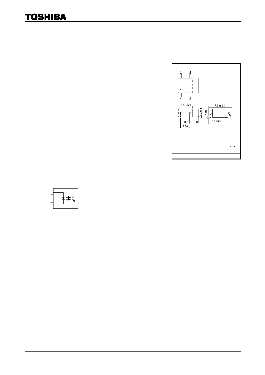
Pin Configurations
(top view)
6
4
3
1
1 : Anode
3 : Cathode
4 : Emitter
6 : Collector
TOSHIBA 11
-4C1
Weight: 0.09g
Unit in mm

TLP124
2002-09-25
2
Current Transfer Ratio
Current Transfer Ratio (min.)
Ta = 25∞C
Ta =
-25~75∞C
Classification
I
F
= 1mA
V
CE
= 0.5V
I
F
= 0.5mA
V
CE
= 1.5V
I
F
= 1mA
V
CE
= 0.5V
Marking Of
Classification
Rank BV
200%
100%
100%
BV
Standard 100% 50%
50% BV,
Blank
(Note) Application type name for certification test, please use standard product type name, i. e.
TLP124 (BV): TLP124
Maximum Rations
(Ta = 25∞C)
Characteristic Symbol
Rating Unit
Forward current
I
F
50
mA
Forward current derating
I
F
/ ∞C
-0.7 (Ta 53∞C)
mA / ∞C
Peak forward current
(100µs pulse, 100pps)
I
FP
1
A
Reverse voltage
V
R
5
V
LE
D
Junction temperature
T
j
125
∞C
Collector
-emitter voltage
V
CEO
80 V
Emitter
-collector valtage
V
ECO
7 V
Collector current
I
C
50
mA
Peak collector current
(10ms pulse, 100pps)
I
CP
100
mA
Power dissipation
P
C
150
mW
Power dissipation derating
(Ta 25∞C)
P
C
/ ∞C
-1.5
mA / ∞C
Det
e
c
t
or
Junction temperature
T
j
125
∞C
Storage temperature range
T
stg
-55~125 ∞C
Operating temperature range
T
opr
-55~100 ∞C
Lead soldering temperature (10s)
T
sol
260
∞C
Total package power dissipation
P
T
200
mW
Total package power dissipation
derating (Ta 25∞C)
P
T
/ ∞C
-2.0 mW
/
∞C
Isolation voltage
(AC, 1min., R.H. 60%)
(Note 1)
BV
S
3750
Vrms
(Note 1) Device considered a two terminal device: Pins1, 3 shorted together and pins 4, 6 shorted together.

TLP124
2002-09-25
3
Recommended Operating Conditions
Characteristic Symbol
Min.
Typ.
Max.
Unit
Supply voltage
V
CC
5 48 V
Forward current
I
F
1.6 20 mA
Collector current
I
C
1 10 mA
Operating temperature
T
opr
-25
75 ∞C
Individual Electrical Characteristics
(Ta = 25∞C)
Characteristic Symbol
Test
Condition
Min.
Typ.
Max.
Unit
Forward voltage
V
F
I
F
= 10 mA
1.0
1.15
1.3
V
Reverse Current
I
R
V
R
=
5 V
10 µA
LE
D
Capacitance C
T
V = 0, f = 1 MHz
30 pF
Collector
-emitter
breakdown voltage
V
(BR) CEO
I
C
= 0.5 mA
80
V
Emitter
-collector
breakdown voltage
V
(BR) ECO
I
E
= 0.1 mA
7
V
V
CE
= 48 V
10 100
nA
Collector dark current
I
D
V
CE
= 48 V, Ta = 85∞C
2 50 µA
Det
e
c
t
or
Capacitance collector to emitter
C
CE
V = 0, f = 1 MHz
12 pF
Coupled Electrical Characteristics
(Ta = 25∞C)
Characteristic Symbol
Test
Condition
MIn.
Typ.
Max.
Unit
100
1200
Current transfer ratio
I
C
/ I
F
I
F
= 1mA, V
CE
= 0.5 V
Rank BV
200
1200
%
50
Low input CTR
I
C
/ I
F (low)
I
F
= 0.5 mA, V
CE
= 1.5 V
Rank BV
100
%
I
C
= 0.5 mA, I
F
= 1 mA
0.4
0.2
Collector
-emitter
saturation voltage
V
CE (sat)
I
C
= 1 mA, I
F
= 1 mA
Rank BV
0.4
V
Off
-state collector current
I
C(off)
V
F
= 0.7V, V
CE
= 48 V
10 µA
Coupled Electrical Characteristics
(Ta =
-
-
-
-
25~75∞C)
Characteristic Symbol
Test
Condition
Min.
Typ.
Max.
Unit
50
%
Current transfer ratio
I
C
/ I
F
I
F
= 1mA, V
CE
= 0.5 V
Rank BV
100
%
50 %
Low input CTR
I
C
/ I
F (low)
I
F
= 0.5 mA, V
CE
= 1.5 V
Rank BV
100 %

TLP124
2002-09-25
4
Isolation Characteristics
(Ta = 25∞C)
Characteristic Symbol
Test
Condition
Min.
Typ.
Max.
Unit
Capacitance
(input to output)
C
S
V
S
= 0, f = 1 MHz
0.8 pF
Isolation resistance
R
S
V
S
= 500 V, R.H. 60%
5◊10
10
10
14
AC, 1 minute
3750
--
AC, 1 s, in oil
10000
V
rms
Isolation voltage
BV
S
DC, 1 minute, in oil
10000
V
dc
Switching Characteristics
(Ta = 25∞C)
Characteristic Symbol
Test
Condition
Min.
Typ.
Max.
Unit
Rise time
t
r
8
Fall time
t
f
8
Turn
-on time
t
ON
10
Turn
-off time
t
OFF
V
CC
= 10 V, I
C
= 2 mA
R
L
= 100
8
µs
Turn
-on time
t
ON
10
Storage time
t
s
50
Turn
-off time
t
OFF
R
L
= 4.7 k
(Fig.1)
V
CC
= 5 V, I
F
= 1.6 mA
300
µs
Fig. 1 Switching time test circuit
V
CC
V
CE
I
F
t
ON
t
OFF
t
s
4.5V
0.5V
I
F
V
CC
V
CE
R
L

TLP124
2002-09-25
5
I
F
≠ Ta
Ambient temperature Ta (∞C)
A
l
l
o
wabl
e f
o
rward
c
u
rrent
I
F
(
mA
)
0
100
-20
80
60
40
20
0 20 40 60 80
120
100
P
C
≠ Ta
Ambient temperature Ta (∞C)
A
l
l
o
wabl
e c
o
l
l
e
c
t
or
power
di
s
s
i
p
at
i
o
n
P
C
(m
W)
200
0
-20
160
120
80
40
0 20 40 60 80
120
100
DV
F
/
DTa ≠ I
F
Forward current I
F
(mA)
Forward v
o
l
t
age
t
e
m
perat
ure
c
oef
f
i
c
i
ent
D
V
F
/
D
Ta
(
m
V
/
∞
C
)
-3.2
-0.4
0.1
-0.8
-2.8
-2.0
-1.6
-1.2
0.3
-2.4
1 5
50
0.5 3
10
30
I
FP
≠ D
R
Duty cycle ratio D
R
P
u
l
s
e
f
o
rward
c
u
rrent
I
FP
(mA
)
3000
10
3
30
1000
300
100
50
10
-3
500
10
-2
10
-1
10
0
3 3 3
Pulse width 100
ms
Ta = 25∞C
I
F
≠ V
F
Forward voltage V
F
(V)
Forward c
u
rrent
I
F
(m
A
)
100
0.1
0.6
50
5
1
0.5
0.8 1.0 1.2
1.4
1.6 1.8
30
10
3
0.3
Ta = 25∞C
I
FP
≠ V
FP
Pulse forward voltage V
FP
(V)
P
u
l
s
e
f
o
rward
c
u
rrent
I
FP
(m
A
)
1000
1.0 1.4 1.8
2.2 2.6 3.0
1
0.6
500
300
100
50
30
10
5
Pulse width 10
ms
Repetitive
Frequency = 100Hz
Ta = 25∞C
3