TLP202A
2002-04-23
1
TOSHIBA Photocoupler Photorelay
TLP202A
Telecommunications
Measurement and Control Equipment
Data Acquisition System
Measurement Equipment
The Toshiba TLP202A consists of a gallium arsenide infrared emitting
diode optically coupled to a photo-MOSFET in an 8-pin SOP package.
This photorelay has higher output current rating than
phototransistor-type photocoupler; hence, it is suitable for use as On/Off
control for high current.
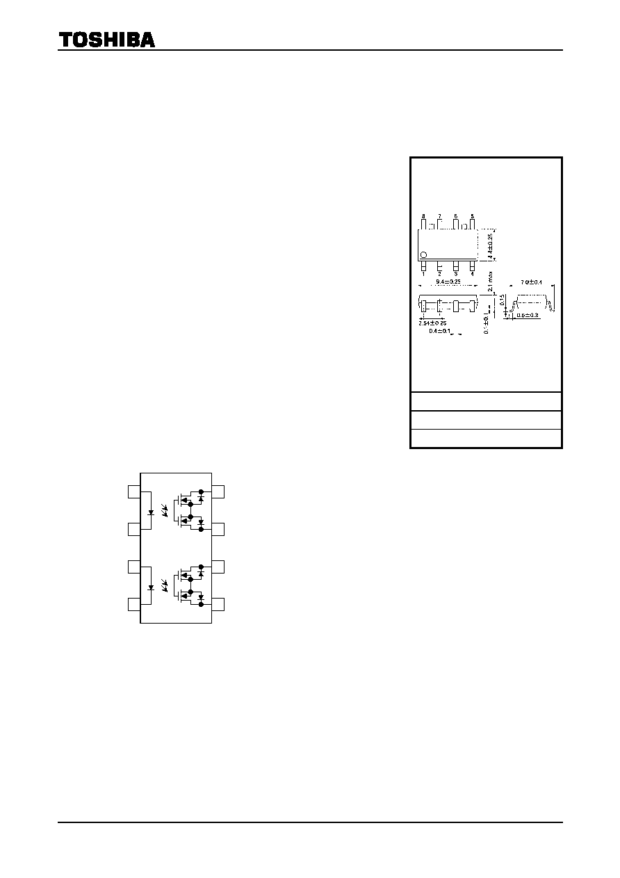
· 8-pin SOP (2.54SOP8): Height = 2.1 mm, pitch = 2.54 mm
· Normally open (1-form-A) device
· Peak off-state voltage: 60 V (min)
· Trigger LED current: 3 mA (max)
· On-state current: 400 mA (max)
· On-state resistance: 2 (max)
· Isolation voltage: 1500 Vrms (min)
· UL recognized: UL1557, File No.E67349
Pin Configuration
(top view)
Unit: mm
JEDEC
JEITA
TOSHIBA 11-10H1
Weight: 0.2 g (typ.)
1
2
8
7
1, 3 : Anode
2, 4 : Cathode
5 :
Drain
D1
6 :
Drain
D2
7 :
Drain
D3
8 :
Drain
D4
3
4
6
5

TLP202A
2002-04-23
2
Maximum Rating
(Ta
=
=
=
=
25°C)
Characteristics Symbol
Rating
Unit
Forward current
I
F
50
mA
Forward current derating
(Ta >
= 25°C)
DI
F
/°C
-0.5 mA/°C
Peak forward current
(100
ms pulse, 100 pps)
I
FP
1
A
Reverse voltage
V
R
5
V
LED
Junction temperature
T
j
125
°C
Off-state output terminal
voltage
V
OFF
60 V
On-state current
I
ON
400
mA
Forward current derating
(Ta >
= 25°C)
DI
ON
/°C
-4.0 mA/°C
Detector
Junction temperature
T
j
125
°C
Storage temperature
T
stg
-55 to 125
°C
Operating temperature
T
opr
-40 to 85
°C
Lead soldering temperature (10 s)
T
sol
260
°C
Isolation voltage
(AC, 1 min, R.H. <
= 60%)
(Note
1)
BV
S
1500
Vrms
Note 1: LED pins are shorted together. Detector pins are also shorted together.
Recommended Operating Conditions
Characteristics Symbol
Min
Typ.
Max
Unit
Supply voltage
V
DD
¾
¾ 48 V
Forward current
I
F
5
7.5
25
mA
On-state current
I
ON
¾
¾ 400
mA
Operating temperature
T
opr
-20
¾ 65 °C
Electrical Characteristics
(Ta
=
=
=
=
25°C)
Characteristics Symbol
Test
Condition
Min
Typ.
Max
Unit
Forward voltage
V
F
I
F
= 10 mA
1.0
1.15
1.3
V
Reverse current
I
R
V
R
= 5 V
¾
¾ 10 mA
LED
Capacitance C
T
V
= 0, f = 1 MHz
¾ 30 ¾ pF
Off-state current
I
OFF
V
OFF
= 60 V
¾
¾ 1 mA
Detector
Capacitance C
OFF
V
= 0, f = 1 MHz
¾ 130 ¾ pF
Coupled Electrical Characteristics
(Ta
=
=
=
=
25°C)
Characteristics Symbol
Test
Condition
Min
Typ.
Max
Unit
Trigger LED current
I
FT
I
ON
= 400 mA
¾ 1.6 3 mA
Return LED current
I
FC
I
OFF
= 100 mA 0.1
¾
¾ mA
On-state resistance
R
ON
I
ON
= 400 mA, I
F
= 5 mA
¾ 1 2 W
TLP202A
2002-04-23
3
Isolation Characteristics
(Ta
=
=
=
=
25°C)
Characteristics Symbol
Test
Condition
Min
Typ.
Max
Unit
Capacitance input to output
C
S
V
S
= 0 V, f = 1 MHz
¾ 0.8 ¾ pF
Isolation resistance
R
S
V
S
= 500 V, R.H. <= 60% 5
´ 10
10
10
14
¾
W
AC, 1 min
1500
¾
¾
AC, 1 s, in oil
¾ 3000 ¾
Vrms
Isolation voltage
BV
S
DC, 1 min, in oil
¾ 3000 ¾ Vdc
Switching Characteristics
(Ta
=
=
=
=
25°C)
Characteristics Symbol
Test
Condition
Min
Typ.
Max
Unit
Turn-on time
t
ON
¾ 0.8 2
Turn-off time
t
OFF
R
L
= 200 W
(Note 2)
V
DD
= 20 V, I
F
= 5 mA
¾ 0.1 0.5
ms
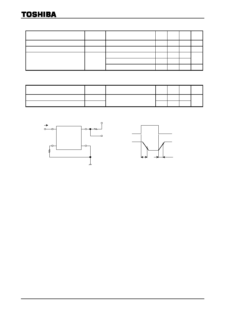
Note 2: Switching time test circuit
t
OFF
t
ON
10%
90%
V
OUT
I
F
6, 8
1, 3
V
DD
V
OUT
R
L
5, 7
2, 4
I
F
TLP202A
2002-04-23
4
· TOSHIBA is continually working to improve the quality and reliability of its products. Nevertheless, semiconductor
devices in general can malfunction or fail due to their inherent electrical sensitivity and vulnerability to physical
stress. It is the responsibility of the buyer, when utilizing TOSHIBA products, to comply with the standards of
safety in making a safe design for the entire system, and to avoid situations in which a malfunction or failure of
such TOSHIBA products could cause loss of human life, bodily injury or damage to property.
In developing your designs, please ensure that TOSHIBA products are used within specified operating ranges as
set forth in the most recent TOSHIBA products specifications. Also, please keep in mind the precautions and
conditions set forth in the "Handling Guide for Semiconductor Devices," or "TOSHIBA Semiconductor Reliability
Handbook" etc..
· The TOSHIBA products listed in this document are intended for usage in general electronics applications
(computer, personal equipment, office equipment, measuring equipment, industrial robotics, domestic appliances,
etc.). These TOSHIBA products are neither intended nor warranted for usage in equipment that requires
extraordinarily high quality and/or reliability or a malfunction or failure of which may cause loss of human life or
bodily injury ("Unintended Usage"). Unintended Usage include atomic energy control instruments, airplane or
spaceship instruments, transportation instruments, traffic signal instruments, combustion control instruments,
medical instruments, all types of safety devices, etc.. Unintended Usage of TOSHIBA products listed in this
document shall be made at the customer's own risk.
· Gallium arsenide (GaAs) is a substance used in the products described in this document. GaAs dust and fumes
are toxic. Do not break, cut or pulverize the product, or use chemicals to dissolve them. When disposing of the
products, follow the appropriate regulations. Do not dispose of the products with other industrial waste or with
domestic garbage.
· The information contained herein is presented only as a guide for the applications of our products. No
responsibility is assumed by TOSHIBA CORPORATION for any infringements of intellectual property or other
rights of the third parties which may result from its use. No license is granted by implication or otherwise under
any intellectual property or other rights of TOSHIBA CORPORATION or others.
· The information contained herein is subject to change without notice.
000707EAC
RESTRICTIONS ON PRODUCT USE