 | –≠–ª–µ–∫—Ç—Ä–æ–Ω–Ω—ã–π –∫–æ–º–ø–æ–Ω–µ–Ω—Ç: TLP227GA | –°–∫–∞—á–∞—Ç—å:  PDF PDF  ZIP ZIP |

TLP227GA, TLP227GA-2
2002-03-13
1
TOSHIBA
Photocoupler
Photo
Relay
TLP227GA, TLP227GA-2
Modem
Telecommunications
PBXs
The Toshiba TLP227GA series consist of a gallium arsenide
infrared-emitting diode optically coupled to a photo-MOSFET in a 4-pin
DIP or a 8-pin DIP package, and has a peak off-State voltage of 400 V.
∑ Normally off function
∑ TLP227GA
: DIP4 (1 form A)
TLP227GA-2
: DIP8 (2 form A)
∑ Peak off-state voltage : 400 V (min)
∑ Trigger LED current
: 3 mA (max)
∑ On-state current
: 120 mA (max)
∑ On-state resistance
: 35 (max)
∑ Isolation voltage
: 2500 Vrms (min)
Pin Configuration (top view)
Unit: mm
JEDEC
JEITA
TOSHIBA 11-5B2
Weight: 0.26 g (typ.)
JEDEC
JEITA
TOSHIBA 11-10C4
Weight: 0.54 g (typ.)
1
2 3
4
TLP227GA
1: Anode
2: Cathode
3: Drain
4: Drain
1
2
3
4
8
7
6
5
1, 3 : Anode
2, 4 : Cathode
5 : Drain D1
6 : Drain D2
7 : Drain D3
8 : Drain D4
TLP227GA-2

TLP227GA, TLP227GA-2
2002-03-13
2
Maximum Rating
(Ta
=
=
=
=
25∞C)
Characteristic Symbol
Rating
Unit
Forward current
I
F
50
mA
Forward current derating
(Ta >
= 25∞C)
DI
F
/∞C
-0.5 mA/∞C
Peak forward current
(100
ms pulse, 100 pps)
I
FP
1
A
Reverse voltage
V
R
5
V
Led
Junction temperature
T
j
125
∞C
Off-state output terminal voltage
V
OFF
400 V
TLP227GA
One
channel
On-state
current
TLP227GA-2
Both
channel
I
ON
120
Ma
TLP227GA
One
channel
On-state
current
rating
(Ta >
= 25∞C)
TLP227GA-2
Both
channel
DI
ON
/∞C
-1.2 mA/∞C
Det
e
c
t
or
Junction temperature
T
j
125
∞C
Storage temperature range
T
stg
-55~125 ∞C
Operating temperature range
T
opr
-40~85 ∞C
Lead soldering temperature (10 s)
T
sol
260
∞C
Isolation voltage (AC, 1 min., R.H. <
= 60%)
(Note 1)
BV
S
2500
Vrms
Note 1: LED pins are shorted together. Detector pins are also shorted together.
Recommended Operating Conditions
Characteristic Symbol
Min
Typ.
Max
Unit
Supply voltage
V
DD
æ
æ 320
V
Forward current
I
F
5 7.5 25 mA
On-state current
I
ON
æ
æ 100
mA
Operating temperature
T
opr
-20
æ 65 ∞C
Individual Electrical Characteristics
(Ta
=
=
=
=
25∞C)
Characteristic Symbol Test
Condition Min
Typ.
Max
Unit
Forward voltage
V
F
I
F
= 10 mA
1.0
1.15
1.3
V
Reverse current
I
R
V
R
= 5 V
æ
æ
10
mA
Led
Capacitance C
T
V
= 0, f = 1 MHz
æ
30
æ
pF
Off-state current
I
OFF
V
OFF
= 400 V
æ
æ
1
mA
Det
e
c
t
or
Capacitance C
OFF
V
= 0, f = 1 MHz
æ
æ
æ
pF

TLP227GA, TLP227GA-2
2002-03-13
3
Coupled Electrical Characteristics
(Ta
=
=
=
=
25∞C)
Characteristic Symbol Test
Condition Min
Typ.
Max
Unit
Trigger LED current
I
FT
I
ON
= 120 mA
æ
1 3 mA
On-state resistance
R
ON
I
ON
= 120 mA, I
F
= 5 mA
æ
18 35
W
Isolation Characteristics
(Ta
=
=
=
=
25∞C)
Characteristic Symbol Test
Condition Min
Typ.
Max
Unit
Capacitance input to output
C
S
V
S
= 0 V, f = 1 MHz
æ 0.8 æ pF
Isolation resistance
R
S
V
S
= 500 V, R.H. <= 60% 5
¥ 10
10
10
14
æ
W
AC, 1 min
2500
æ
æ
AC, 1 s (in oil)
æ 5000 æ
Vrms
Isolation voltage
BV
S
DC, 1 min (in oil)
æ 5000 æ Vdc
Switching Characteristics
(Ta
=
=
=
=
25∞C)
Characteristic Symbol Test
Condition Min
Typ.
Max
Unit
Turn-on time
t
ON
æ
æ 1
Turn-off time
t
OFF
R
L
= 200 W
V
DD
= 20 V, I
F
= 5 mA
(Note 2)
æ
æ 1
ms
Note 2: Switching time test circuit
TLP227GA
V
DD
R
L
2
1
I
F
3
4
V
OUT
V
OUT
I
F
t
ON
t
OFF
90%
10%
TLP227GA-2
V
DD
R
L
2
1
I
F
7
8
V
OUT

TLP227GA, TLP227GA-2
2002-03-13
4
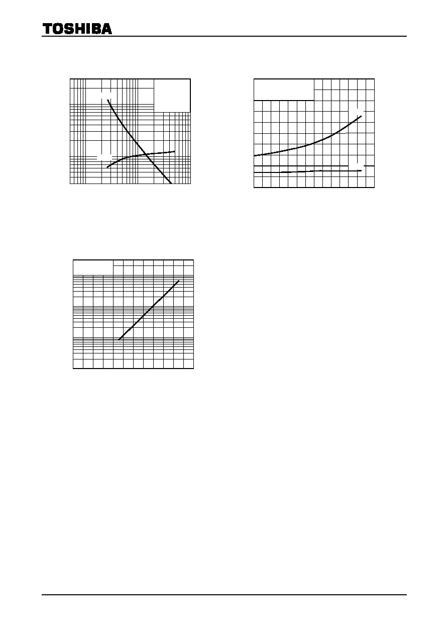
On-
s
t
a
t
e
r
e
sis
t
a
n
ce
R
ON
(
W
)
On-s
t
a
t
e
c
u
r
r
en
t I
ON
(
m
A
)
Ambient temperature Ta (∞C)
I
F
≠ Ta
A
l
l
o
w
abl
e fo
rw
a
r
d
cu
rre
nt
I
F
(
m
A
)
Ambient temperature Ta (∞C)
I
ON
≠ Ta
On-s
t
a
t
e
c
u
r
r
en
t I
ON
(
m
A
)
Forward voltage V
F
(V)
I
F
≠ V
F
Fo
rw
ar
d
c
u
r
r
en
t I
F
(m
A
)
On-state voltage V
ON
(V)
I
ON
≠ V
ON
Ambient temperature Ta (∞C)
R
ON
≠ Ta
Ambient temperature Ta (∞C)
I
FT
≠ Ta
T
r
i
g
ge
r l
e
d cu
rr
ent
I
FT
(mA
)
0
-20
20
40
60
80
100
0 20 40 60 80 100 120
0
-20
0 20 40 60 80 100 120
40
80
120
160
200
240
280
-200
-3
-100
0
100
200
-2
-1 0 1 2 3
Ta
= 25∞C
IF = 5 mA
0
-20
0
20
40
60
80
100
10
20
30
40
50
60
ION = 120 mA
IF = 5 mA
t
< 1 s
0
-40
-20 0 20 40 60 80 100
1
2
3
4
5
ION = 120 mA
t
< 1 s
0.1
0.6 0.8 1 1.2 1.4 1.6 1.8
1
10
100
0.3
3
30
Ta
= 25∞C
TLP227GA, TLP227GA-2
2002-03-13
5
0.1
-20 0 20 40 60 80 100
0.3
1
3
10
300
VOFF = 400 V
30
100
t
ON
, t
OFF
≠ Ta
I
OFF
≠ Ta
Input current I
F
(mA)
Ambient temperature Ta (∞C)
Ambient temperature Ta (∞C)
Switch
in
g
ti
m
e
t
ON
, t
OFF
(
m
s)
Switch
in
g
ti
m
e
t
ON
, t
OFF
(
m
s)
Of
f-s
t
at
e
c
u
r
r
en
t I
OFF
(
n
A
)
t
ON
, t
OFF
≠ I
F
tON
tOFF
VDD = 20 V, RL = 200 W
IF = 5 mA
0
-20 0 20 40 60 80 100
-40
1000
800
600
400
200
3000
1000
300
100
500
30
50
0.5 1
3 5 10
30
100
50
Ta
= 25∞C
IF = 5 mA
VDD = 20 V
RL = 200 W
tOFF
tON