 | ÐлекÑÑоннÑй компоненÑ: TLP512 | СкаÑаÑÑ:  PDF PDF  ZIP ZIP |
Äîêóìåíòàöèÿ è îïèñàíèÿ www.docs.chipfind.ru
TLP512
2002-11-28
1
TOSHIBA
Photocoupler
GaAAs IRED + Photo IC
TLP512
Digital Logic Ground Isolation
Line Receiver
Microprocessor System Interfaces
Switching Power Supply Feedback Control
Transistor Inverter
The TLP512 consists of a GaAAs high-output light emitting diode and a
high-speed detector that contains a PN photodiode and an amplifier
transistor into a single chip.
· Isolation voltage: 2500 Vrms (min)
· Switching speed: t
pHL
= 0.8 µs, t
pLH
= 0.8 µs (max)
@R
L
= 1.9 k
· TTL compatible
· UL recognized: UL1577, file No. E67349
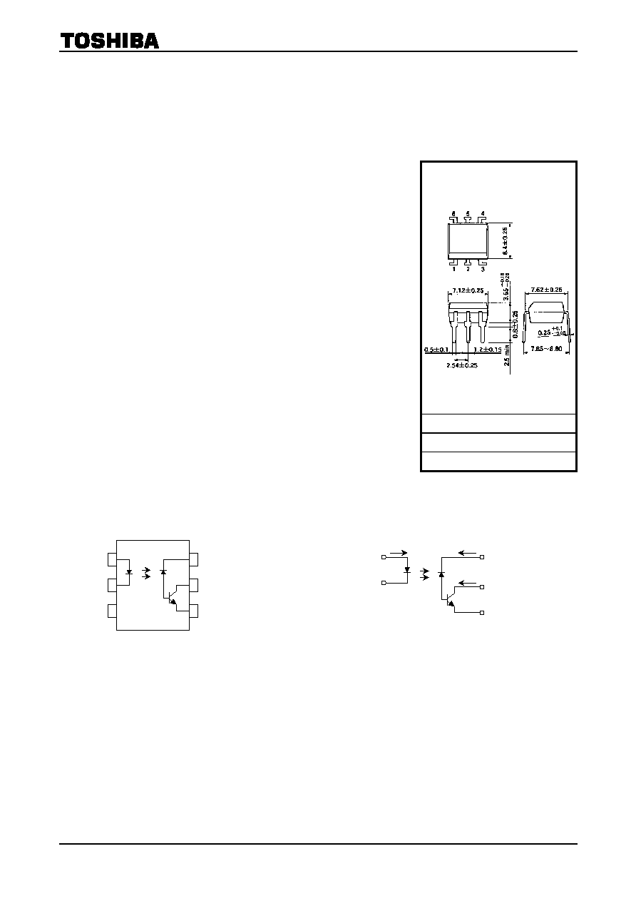
Pin Configuration
(top view)
Schematic
Unit: mm
JEDEC
JEITA
TOSHIBA 11-7A8
Weight: 0.4 g (typ.)
1
2
I
F
I
CC
I
O
6
5
4
V
CC
V
O
GND
V
F
1: Anode
2: Cathode
3: NC
4: Emitter (GND)
5: Collector (OUT)
6: V
CC
1
3
6
4
2
5
TLP512
2002-11-28
2
Maximum Ratings
(Ta
=
=
=
=
25°C)
Characteristics Symbol
Rating
Unit
DC forward current
(Note 1)
I
F
25 mA
Pulse forward current
(Note 2)
I
FP
50 mA
Peak transient forward current
(Note 3)
I
FPT
1 A
DC reverse voltage
V
R
5 V
LE
D
Diode power dissipation
(Note 4)
P
D
45 mW
Output current
I
O
8 mA
Peak output current
I
OP
16 mA
Output voltage
V
O
-0.5 to 15
V
Supply voltage
V
CC
-0.5 to 15
V
Det
e
c
t
or
Output power dissipation
(Note 5)
P
o
100
mW
Operating temperature range
T
opr
-55 to 100
°C
Storage temperature range
T
stg
-55 to 125
°C
Soldering temperature (10 s)
(Note 6)
T
sol
260 °C
Isolation voltage (R.H.
£ 60%, AC 1 min)
(Note 7)
BV
S
2500 Vrms
Note 1: Decreases at the rate of 0.8 mA/
°C with the ambient temperature of 70°C or higher.
Note 2: Duty cycle of 50%, pulse width of 1 ms.
Decreases at the rate of 1.6 mA/
°C with the ambient temperature of 70°C or higher.
Note 3: Pulse width
£ 1 ms, 300 pps
Note 4: Decreases at the rate of 0.9 mW/
°C with the ambient temperature of 70°C or higher.
Note 5: Decreases at the rate of 2 mW/
°C with the ambient temperature of 70°C or higher.
Note 6: Soldering is performed 2 mm from the bottom of the package.
Note 7: Device considered a two-terminal device: pins 1, 2, and 3 shorted together and pins 4, 5 and 6 shorted
together.
TLP512
2002-11-28
3
Electrical Characteristics
(Ta
=
=
=
=
25°C)
Characteristic Symbol
Test
Condition
Min
Typ.
Max
Unit
Forward voltage
V
F
I
F
= 16 mA
¾ 1.65 1.85
V
Forward voltage temperature
coefficient
DV
F
/
DTa I
F
= 16 mA
¾
-2
¾ mV/°C
Reverse current
I
R
V
R
= 5 V
¾
¾ 10 mA
LE
D
Pin-to-pin capacitance
C
T
V
F
= 0, f = 1 MHz
¾ 4.5 ¾ pF
I
OH (1)
I
F
= 0 mA, V
CC
= V
O
= 5.5 V
¾ 3 500
nA
I
OH (2)
I
F
= 0 mA, V
CC
= V
O
= 15 V
¾
¾ 5
High-level output current
I
OH
I
F
= 0 mA, V
CC
= V
O
= 15 V
Ta
= 70°C
¾
¾ 50
mA
Det
e
c
t
or
High-level supply current
I
CCH
I
F
= 0 mA, V
CC
= 15 V
¾ 0.01 1 mA
Coupled Electrical Characteristics
(Ta
=
=
=
=
25°C)
Characteristic Symbol
Test
Condition
Min
Typ.
Max
Unit
I
F
= 16 mA, V
CC
= 4.5 V
V
O
= 0.4 V
20 40
¾
Current transfer ratio
I
O
/I
F
I
F
= 16 mA, V
CC
= 4.5 V
V
O
= 0.4 V, Ta = 0 to 70°C
15
¾
¾
%
Low-level output voltage
V
OL
I
F
= 16 mA, V
CC
= 4.5 V
I
O
= 2.4 mA
¾
¾ 0.4 V
Isolation Characteristics
(Ta
=
=
=
=
25°C)
Characteristic Symbol
Test
Condition
Min
Typ.
Max
Unit
Capacitance input to output
C
S
V
S
= 0, f = 1 MHz
(Note 7)
¾ 0.8 ¾ pF
Isolation resistance
R
S
R.H.
£ 60%, V
S
= 500 V (Note 7) 5 ´ 10
10
10
14
¾
W
AC 1 min
2500
¾
¾
AC 1 s, in oil
¾ 5000 ¾
Vrms
Isolation voltage
BV
S
DC 1 min, in oil
¾ 5000 ¾
V
dc
TLP512
2002-11-28
4
Switching Characteristics
(Ta
=
25°C)
Characteristics Symbol
Test
Circuit
Test Condition
Min
Typ.
Max
Unit
Propagation delay time (H
® L)
t
pHL
I
F
= 0 ® 16 mA, R
L
= 1.9 kW
¾
¾ 0.8 ms
Propagation delay time (L
® H)
t
pLH
1
I
F
= 16 ® 0 mA, R
L
= 1.9 kW
¾
¾ 0.8 ms
Common mode transient immunity at
logic high output
(Note 8)
CM
H
I
F
= 0 mA, V
CM
= 200 V
P-P
R
L
= 1.9 kW
¾ 1500 ¾ V/ms
Common mode transient immunity at
logic low output
(Note 8)
CM
L
2
I
F
= 16 mA, V
CM
= 200 V
P-P
R
L
= 1.9 kW
¾
-1500
¾ V/ms
Note 8: Common mode transient immunity in logic high level is the maximum tolerable (positive) dV
CM
/dt on the
leading edge of the common mode pulse, V
CM
, to assure that the output will remain in a logic high state
(V
OUT
> 2.0 V).
Common mode transient immunity in logic low level is the maximum tolerable (negative) dV
CM
/dt on the
trailing edge of the common mode pulse, V
CM
, to assure that the output will remain in a logic low state
(V
OUT
< 0.8 V).
Note 9: Electrostatic discharge immunity (pin to pin): 100 V (max)
(C
£ 200 pF, R = 0)
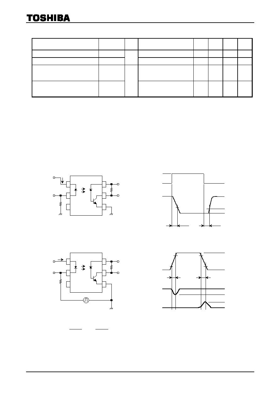
Test Circuit 1: Switching Time Test Circuit
Test Circuit 2: Common Mode Noise Immunity Test Circuit
s)
(
f
t
(V)
160
L
CM
,
s)
(
r
t
(V)
160
H
CM
m
=
m
=
1
3
6
4
2
5
V
CC
= 5 V
V
O
Output monitor
I
F
100
9
R
L
V
CM
Pulse generator
Z
O
= 50 W
V
CM
200 V
V
O
(I
F
= 0 mA)
V
O
(I
F
= 16 mA)
0 V
5 V
2 V
0.8 V
V
OL
10%
90%
tf
tr
t
pHL
1.5 V
5 V
1.5 V
V
OL
t
pLH
V
O
0
I
F
1
3
6
4
2
5
V
CC
= 5 V
V
O
Output monitor
Pulse input
PW
= 100 ms
Duty ratio
= 1/10
I
F
monitor
I
F
100
9
R
L
TLP512
2002-11-28
5
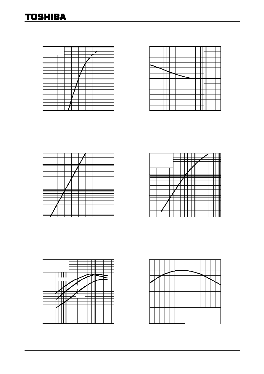
*: The above graphs show typical characteristics.
C
u
rr
ent
tr
ans
fer
r
a
ti
o
I
O
/I
F
(%
)
Outp
ut
cur
r
e
n
t I
O
(
m
A
)
Forward voltage V
F
(V)
I
F
V
F
Fo
rw
ar
d
c
u
r
r
en
t I
F
(m
A
)
Forward current I
F
(mA)
DV
F
/
DTa I
F
Fo
rw
ar
d v
o
l
t
age
te
mp
er
atu
r
e c
o
e
f
fi
ci
e
n
t
D
V
F
/
D
Ta
(
m
V
/
°
C
)
Ambient temperature Ta ()
I
OH
(1) Ta
H
i
gh-l
e
vel
ou
tpu
t
c
u
rr
ent
I
OH
(µA
)
Forward current I
F
(mA)
I
O
I
F
Forward current I
F
(mA)
I
O
/I
F
I
F
Ambient temperature Ta ()
I
O
/I
F
Ta
No
r
m
a
liz
e
d
I
O
/I
F
0.01
1.0 1.2 1.4 1.6 1.8 2.0
0.03
0.1
0.3
1
3
10
30
100
Ta
= 25°C
-1.4
0.1
0.3
1
3 10 30
-1.6
-1.8
-2.0
-2.2
-2.4
-2.6
0.6
0 40 80
120
160
1
3
10
30
100
300
100
VCC = 5 V
VO = 0.4 V
Ta
= 25°C
0.01
0.1
0.3
1
10 30
0.03
0.1
0.3
1
3
10
3
Normalized to: IF = 16 mA
VCC = 4.5 V
VO = 0.4 V
Ta
= 25°C
100
0
-40
-20
0
40 60
20
80
0.2
0.4
0.6
0.8
1.0
1.2
1
0.1 0.3 1
10 30
3
3
10
30
100
VCC = 5 V
VO = 0.4 V
100ºC
Ta
= -25ºC
25ºC