 | –≠–ª–µ–∫—Ç—Ä–æ–Ω–Ω—ã–π –∫–æ–º–ø–æ–Ω–µ–Ω—Ç: TLP550 | –°–∫–∞—á–∞—Ç—å:  PDF PDF  ZIP ZIP |

TLP550
2002-09-25
1
TOSHIBA Photocoupler Infrared LED
+
Photo IC
TLP550
Degital Logic Isolation
Line Receiver Feedback Control
Power Supply Control
Switching Power Supply
Transistor Invertor
TLP550 constructs a high emitting diode and a one chip photo diode-
transistor.
TLP550 has no base connection, and is suitable for application at noisy
environmental condition.
This unit is 8-lead DIP package.
l Isolation voltage: 2500 Vrms (min.)
l Switching speed: t
pHL,
t
pLH
= 0.5µs (typ.)(R
L
=1.9 k)
l TTL compatible
l UL recognized: UL1577, file No. E67349
Pin Configuration
(top view)
1 : N.C.
2 : Anode
3 : Cathode
4 : N.C.
5 : Emitter
6 : Collector
7 : N.C.
8 : Cathode
1
2
6
8
3
5
4
7
Schematic
GND
2
3
6
V
CC
V
O
I
O
5
8
I
CC
I
F
V
F
TOSHIBA 11-10C4
Weight: 0.54 g
Unit in mm

TLP550
2002-09-25
2
Maximum Ratings
(Ta = 25∞C)
Characteristic Symbol
Rating
Unit
Forward current
(Note 1)
I
F
25 mA
Pulse forward current
(Note 2)
I
FP
50 mA
Peak transient forward
current (Note
3)
I
FPT
1 A
Reverse voltage
V
R
5 V
LE
D
Diode power dissipation
(Note
4)
P
D
45 mW
Output current
I
O
8 mA
Peak output current
I
OP
16 mA
Supply voltage
V
CC
-0.5~15 V
Output voltage
V
O
-0.5~15 V
Det
e
c
t
or
Output power dissipation
(Note
5)
P
O
100 mW
Operating temperature range
T
opr
-55~100 ∞C
Storage temperature range
T
stg
-55~125 ∞C
Lead solder temperature (10s)
T
sol
260 ∞C
Isolation voltage
(AC, 1min., R.H. = 40~60%)
(Note 6)
BV
S
2500 Vrms
(Note 1) Derate 0.8mA above 70∞C.
(Note 2) 50% duty cycle, 1ms pulse width.
Derate 1.6mA / ∞C above 70∞C.
(Note 3) Pulse width 1µs, 300pps.
(Note 4) Derate 0.9mW / ∞C above 70∞C.
(Note 5) Derate 2mW / ∞C above 70∞C.

TLP550
2002-09-25
3
Electrical Characteristics
(Ta = 25∞C)
Characteristic Symbol
Test
condition
Min.
Typ.
Max.
Unit
Forward voltage
V
F
I
F
= 16 mA
1.45
1.65
1.85
V
Forward voltage
temperature coefficient
V
F
/Ta I
F
= 16 mA
-2
mV / ∞C
Reverse current
I
R
V
R
= 5 V
10 µA
LE
D
Capacitance between
terminal
C
T
V
F
= 0, f = 1MHz
60 pF
I
OH (1)
I
F
= 0 mA, V
CC
= V
O
= 5.5 V
3 500
nA
I
OH (2)
I
F
= 0 mA, V
CC
= V
O
= 15 V
5 µA
High level output
current
I
OH
I
F
= 0 mA, V
CC
= V
O
= 15 V
Ta = 70∞C
50 µA
Det
e
c
t
or
High level supply
voltage
I
CCH
I
F
= 0 mA, V
CC
= 15 V
0.01 1 µA
Ta = 25∞C
10
30
Rank : 0
19
30
Ta = 0~70∞C
5
Current transfer ratio
I
O
/ I
F
I
F
= 16 mA
V
CC
= 4.5 V
V
O
= 0.4 V
Rank : 0
15
%
Low level output
voltage
V
OL
I
F
= 16 mA, V
CC
= 4.5 V
I
O
= 1.1 mA
(rank 0: I
O
= 2.4mA)
0.4 V
Isolation resistance
R
S
R.H. = 40~60%, V = 1kV DC
(Note
6)
10
12
Coupl
ed
Capacitance between
input to output
C
S
V = 0, f = 1MHz
0.8 pF
Switching Characteristics
(Ta = 25∞C)
Characteristic Symbol Test
Condition Min.
Typ.
Max.
Unit
I
F
= 0 16 mA, V
CC
= 5V, R
L
= 4.1 k
0.3 0.8
Propagation delay time
(H L)
t
pHL
(Note 7) Rank 0: R
L
= 1.9 k
0.5 0.8
µs
I
F
= 16 0 mA, V
CC
= 5V, R
L
= 4.1 k
1.0 2.0
Propagation delay time
(L H)
t
pLH
(Note 7) Rank 0: R
L
= 1.9 k
0.6 1.2
µs
Common mode transient
immunity at high output
level
C
MH
I
F
= 0 mA, V
CM
= 200 V
p
-p
R
L
= 4.1 k (rank 0: R
L
= 1.9 k)
(Note
8)
1500 V
/µs
Common mode transient
immunity at low output
level
C
ML
I
F
= 16 mA, V
CM
= 200 V
p
-p
R
L
= 4.1 k (rank 0: R
L
= 1.9 k)
(Note
8)
-1500
V
/µs
TLP550
2002-09-25
4
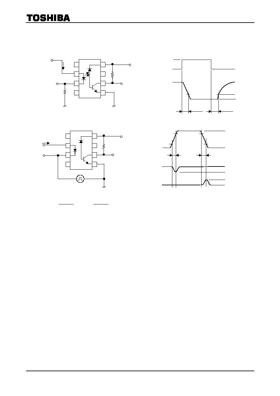
(Note 6) Device considered two
-terminal device: Pins 1, 2, 3 and 4 shorted together and pin 5, 6, 7 and 8 shorted together.
(Note 7) Switching time test circuit.
(Note 8) Common mode transient immunity test circuit.
(Note 9) Maximum electrostatic discharge voltage for any pins: 100V (C = 200pF, R = 0)
V
CC
=5V
V
O
Pulse
input
Output
monitor
R
L
6
4
3
1
5
7
PW = 100µs
Duty ratio = 1 / 10
I
F
monitor
I
F
8
2
51
I
F
V
O
0
5V
1.5V
V
OL
1.5V
t
pHL
t
pLH
V
CM
200V
V
O
(I
F
= 0mA)
V
O
(I
F
= 16mA)
0V
5V
2V
0.8V
V
OL
10%
90%
t
f
t
r
V
CC
=5V
V
O
Output
monitor
R
L
6
4
3
1
5
7
I
F
8
2
V
CM
Pulse gen
Z
O
=50
CM
H
=
CM
L
=
160 (V)
160 (V)
,
t
f
(µs)
t
f
(µs)

TLP550
2002-09-25
5
Fo
rw
ar
d
c
u
r
r
en
t I
F
(m
A
)
Forward voltage VF (V)
I
F
≠ V
F
100
1.0
1
10
0.1
1.2
1.4 1.6 1.8
2.0
0.01
Ta = 25∞C
50
30
5
3
0.5
0.3
0.05
0.03
Fo
rw
ar
d v
o
l
t
ag
e t
e
m
per
atu
r
e
coef
fi
ci
en
t
V
F
/
Ta
(
m
V
/
)
0.1
-2.2
-2.4
-2.6
-1.4
0.5
0.3
-2.0
-1.8
-1.6
1 3 10
5
V
F
/ Ta ≠ I
F
Forward current I
F
(mA)
30
Outp
ut
cur
r
e
n
t I
O
(
m
A
)
l
O
≠ I
F
Forward current I
F
(mA)
0.1
1
3
10
0.01
0.5
0.3
0.3
0.1
0.03
1
30 100
50 300
10
3 5
0.05
0.5
5
VCC = 5V
VO = 0.4V
Ta = 25∞C
Ambient temperature Ta ()
No
r
m
a
liz
e
d
I
O
/
I
F
I
O
/ I
F
≠ Ta
60
40
0
20
-20
-40
0.2
0
80
0.6
0.4
0.8
1.2
1.0
100
Normalized To :
IF = 16mA
VCC = 4.5V
VO = 0.4V
Ta = 25∞C
H
i
gh l
e
vel
out
put
cu
rr
ent
I
OH
(µA
)
Ambient temperature Ta ()
I
OH
(1) ≠ Ta
300
1
100
50
3
10
5
30
0.6
160
120
80
40
0
Forward current IF (mA)
30
I
O
/ I
F
≠ I
F
C
u
rr
ent
tr
ans
fer
r
a
ti
o
I
O
/ I
F
(%
)
100∞C
100
50
10
5
3
1
0.3
1
0.5
3
10 30
50
5
VCC = 5V
VO = 0.4V
Ta =
-
25∞C
25∞C

TLP550
2002-09-25
6
Outp
ut
vol
t
ag
e V
O
(V
)
Forward current I
F
(mA)
V
O
≠ I
F
20
16
8
12
0
4
5
4
0
3
2
1
24
Ta=25∞C
VCC = 5V
R
L
V
O
I
F
3.9k
10k
RL=2k
Load resistance RL (k)
t
pHL
, t
pLH
≠ R
L
P
r
opag
ati
o
n d
e
l
a
y
ti
m
e
t pLH
, t
pH
L (µ
s
)
5
3
1
0.5
0.3
0.1
30
1
3 10
50
100
5
IF = 16mA
VCC = 5V
Ta = 25∞C
t
pLH
t
pHL
Output voltage V
O
(V)
Outp
ut
cur
r
e
n
t I
O
(
m
A
)
I
O
≠ V
O
5
4
2 3
0
1
10
8
0
6
4
2
6
7
VCC = 5V
Ta = 25∞C
20mA
15mA
30mA
IF=5mA
25mA
10mA

TLP550
2002-09-25
7
∑ TOSHIBA is continually working to improve the quality and reliability of its products. Nevertheless, semiconductor
devices in general can malfunction or fail due to their inherent electrical sensitivity and vulnerability to physical
stress. It is the responsibility of the buyer, when utilizing TOSHIBA products, to comply with the standards of safety
in making a safe design for the entire system, and to avoid situations in which a malfunction or failure of such
TOSHIBA products could cause loss of human life, bodily injury or damage to property.
In developing your designs, please ensure that TOSHIBA products are used within specified operating ranges as
set forth in the most recent TOSHIBA products specifications. Also, please keep in mind the precautions and
conditions set forth in the "Handling Guide for Semiconductor Devices," or "TOSHIBA Semiconductor Reliability
Handbook" etc..
∑ The TOSHIBA products listed in this document are intended for usage in general electronics applications (computer,
personal equipment, office equipment, measuring equipment, industrial robotics, domestic appliances, etc.). These
TOSHIBA products are neither intended nor warranted for usage in equipment that requires extraordinarily high
quality and/or reliability or a malfunction or failure of which may cause loss of human life or bodily injury
("Unintended Usage"). Unintended Usage include atomic energy control instruments, airplane or spaceship
instruments, transportation instruments, traffic signal instruments, combustion control instruments, medical
instruments, all types of safety devices, etc.. Unintended Usage of TOSHIBA products listed in this document shall
be made at the customer's own risk.
∑ The information contained herein is presented only as a guide for the applications of our products. No responsibility
is assumed by TOSHIBA CORPORATION for any infringements of intellectual property or other rights of the third
parties which may result from its use. No license is granted by implication or otherwise under any intellectual
property or other rights of TOSHIBA CORPORATION or others.
∑ The information contained herein is subject to change without notice
000707EAA
RESTRICTIONS ON PRODUCT USE