 | ÐлекÑÑоннÑй компоненÑ: TLP599G | СкаÑаÑÑ:  PDF PDF  ZIP ZIP |
Äîêóìåíòàöèÿ è îïèñàíèÿ www.docs.chipfind.ru
TLP599G
2002-09-25
1
TOSHIBA Photocoupler Photo Relay
TLP599G
Telecommunication
Data Acquisition
Measurement Instrumentation
The TOSHIBA TLP599G consists of a gallium arsenide infrared emitting
diode optically coupled to a photo-MOS FET in a six lead plastic DIP
package (DIP6).
The TLP599G is a bi-directional switch which can replace mechanical
relays in many applications.
· Peak off-state voltage: 400V (min.)
· On-state current: 120mA (max.) (A connection)
· On-state resistance: 30 (max.) (A connection)
· Insulation thickness: 0.4mm (max.)
· Isolation voltage: 2500Vrms (min.)
· UL recognized: UL1577, file no. E67349
· Trigger LED current (Ta = 25°C)
Trigger LED Current
(mA)
@I
ON
= 120mA
Classification
(Note
1)
Min. Max.
Marking Of
Classification
(IFT2) -- 2
T2
Standard -- 5
T2,
blank
(Note 1): Application type name for certification
test, please use standard product type
name, i.e.
TLP599G (IFT2) :TLP599G
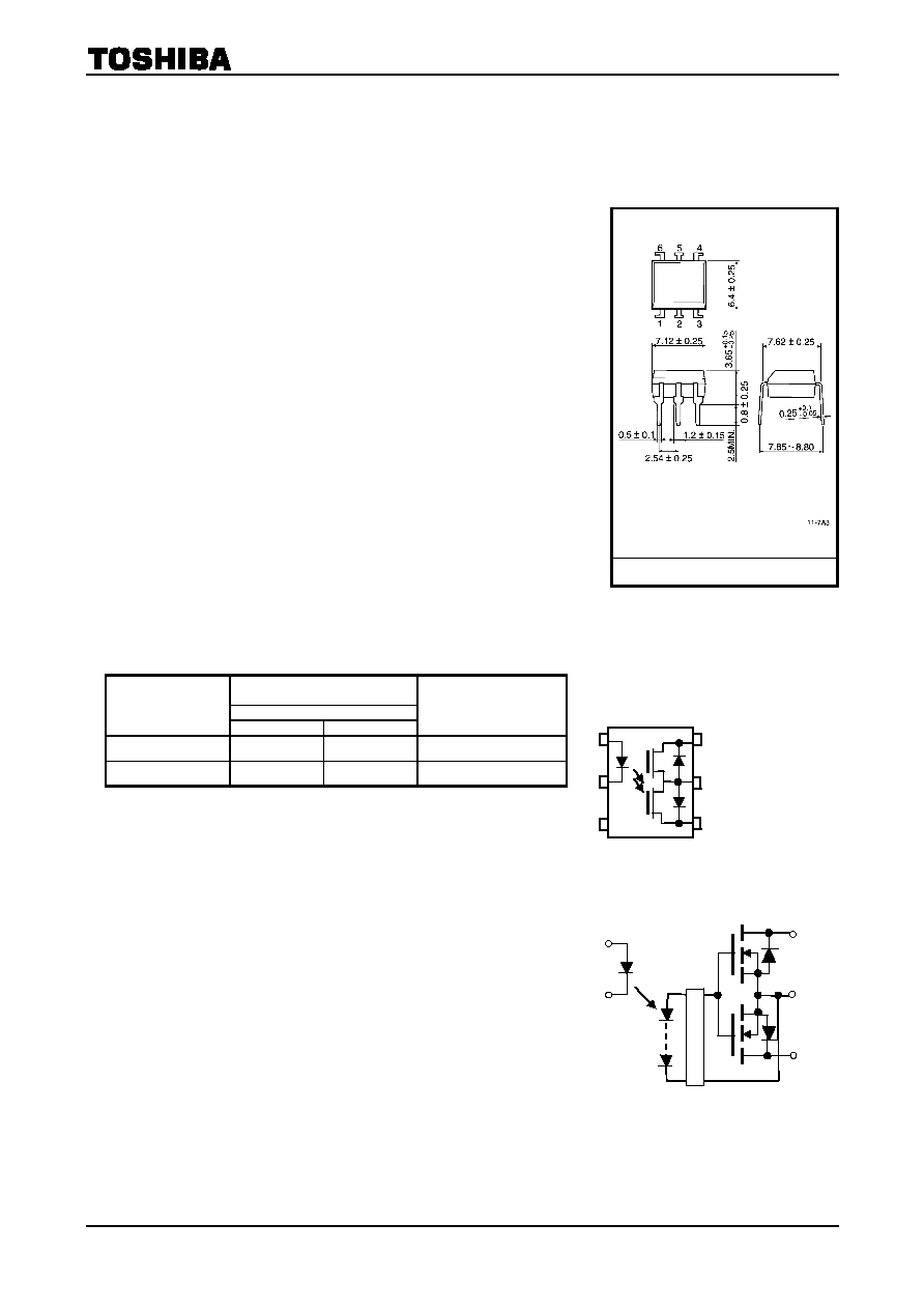
Pin Configuration
(top view)
1 : Anode
2 : Cathode
3 : NC
4 : Drain D1
5 : Source
6 : Drain D2
1
3
6
4
2
5
Schematic
2
1
6
5
4
Unit in mm
TOSHIBA 11
-7A8
TLP599G
2002-09-25
2
Maximum Ratings
(Ta = 25°C)
Characteristic Symbol
Rating
Unit
Forward current
I
F
50 mA
Forward current derating (Ta 25°C)
I
F
/ °C
-0.5
mA / °C
Peak forward current (100 µs pulse, 100 pps)
I
FP
1 A
Reverse voltage
V
R
5 V
LE
D
Junction temperature
T
j
125 °C
Off
-state output terminal voltage
V
OFF
400
V
A connection
120
B connection
150
On
-state RMS current
C connection
I
ON
200
mA
A connection
-1.2
B connection
-1.5
On
-state current derating (Ta 25°C)
C connection
I
ON
/ °C
-2.0
mA / °C
Det
e
c
t
or
Junction temperature
T
j
125 °C
Storage temperature range
T
stg
-55~125 °C
Operating temperature range
T
opr
-40~85 °C
Lead soldering temperature (10 s)
T
sol
260 °C
Isolation voltage (AC, 1 min., R.H. 60%)
(Note 2)
BV
S
2500 Vrms
(Note 2): Device considered a two
-terminal device: Pins 1, 2 and 3 shorted together, and pins 4, 5 and 6
shorted together.
Recommended Operating Conditions
Characteristic Symbol
Min.
Typ.
Max.
Unit
Supply voltage
V
DD
--
--
320
V
Forward current
I
F
7.5
15
25
mA
On
-state current
I
ON
--
--
120
mA
Operating temperature
T
opr
-20
-- 80 °C
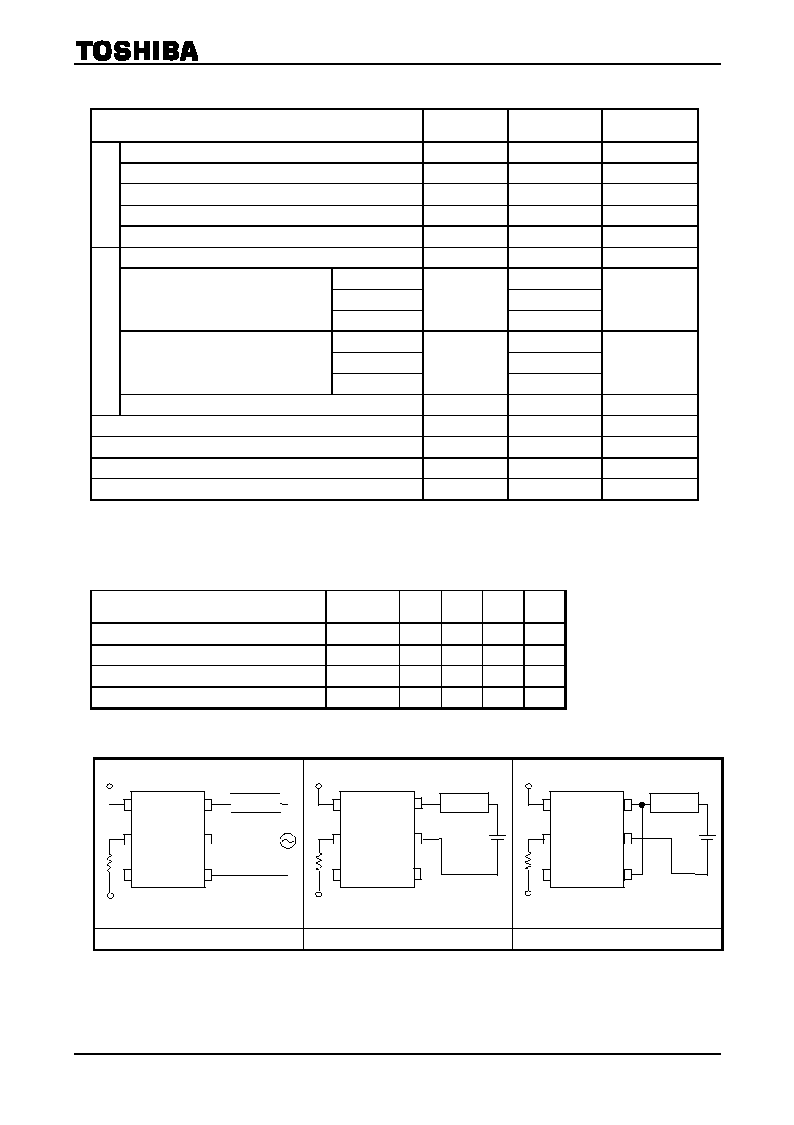
Circuit Connections
1
2
3
6
5
4
LOAD
AC
DC
or
1
2
3
6
5
4
LOAD
DC
1
2
3
6
5
4
LOAD
DC
A connection B connection C connection
TLP599G
2002-09-25
3
Individual Electrical Characteristics
(Ta = 25°C)
Characteristic Symbol
Test
Condition
Min.
Typ.
Max.
Unit
Forward voltage
V
F
I
F
= 10 mA
1.0
1.15
1.3
V
Reverse current
I
R
V
R
= 5V
--
--
10
µA
LE
D
Capacitance C
T
V
= 0, f = 1 MHz
--
30
--
pF
Off
-state current
I
OFF
V
OFF
= 400 V
--
--
1
µA
Det
e
c
t
or
Capacitance C
OFF
V
= 0, f = 1 MHz
--
--
--
pF
Coupled Electrical Characteristics
(Ta = 25°C)
Characteristic Symbol
Test
Condition
Min.
Typ/
Max.
Unit
Trigger LED current
I
FT
I
ON
= 120 mA
--
1
5
mA
A connection
I
ON
= 120 mA, I
F
= 10 mA
--
20
30
B connection
I
ON
= 150 mA, I
F
= 10 mA
--
12
20
On
-state
Resistance
C connection
R
ON
I
ON
= 200 mA, I
F
= 10 mA
--
6
10
Isolation Characteristics
(Ta = 25°C)
Characteristic Symbol
Test
Condition
Min.
Typ.
Max.
Unit
Capacitance input to output
C
S
V
S
= 0, f = 1 MHz
--
0.8
--
pF
Isolation resistance
R
S
V
S
= 500 V, R.H. 60%
5
´ 10
10
10
14
--
AC, 1 minute
2500
--
--
AC, 1 second (in oil)
--
5000
--
Vrms
Isolation voltage
BV
S
DC, 1 minute (in oil)
--
5000
--
V
dc
Switching Characteristics
(Ta = 25°C)
Characteristic Symbol
Test
Condition
Min.
Typ.
Max.
Unit
Turn
-on time
t
on
--
--
2
Turn
-off time
t
off
R
L
= 200
V
DD
= 20 V, I
F
= 10 mA
-- -- 2
ms
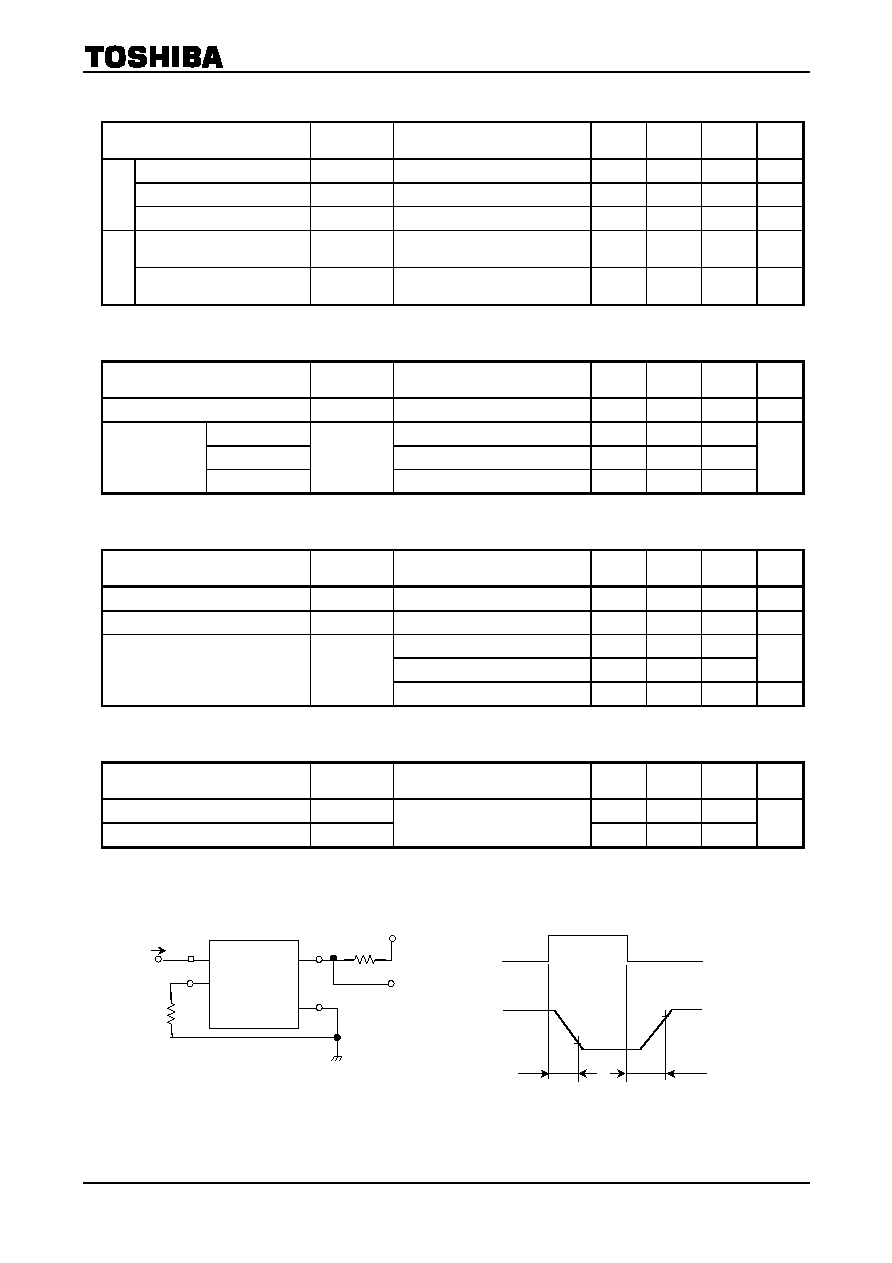
Switching Time Test Circuit
t
off
t
on
10%
90%
V
OUT
I
F
6
1
V
DD
V
OUT
R
L
4
2
I
F
TLP599G
2002-09-25
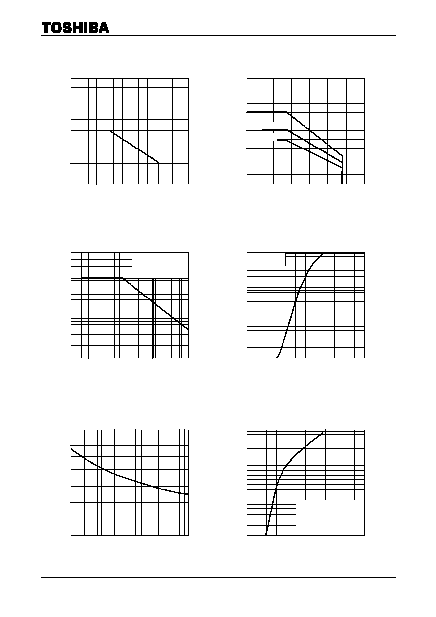
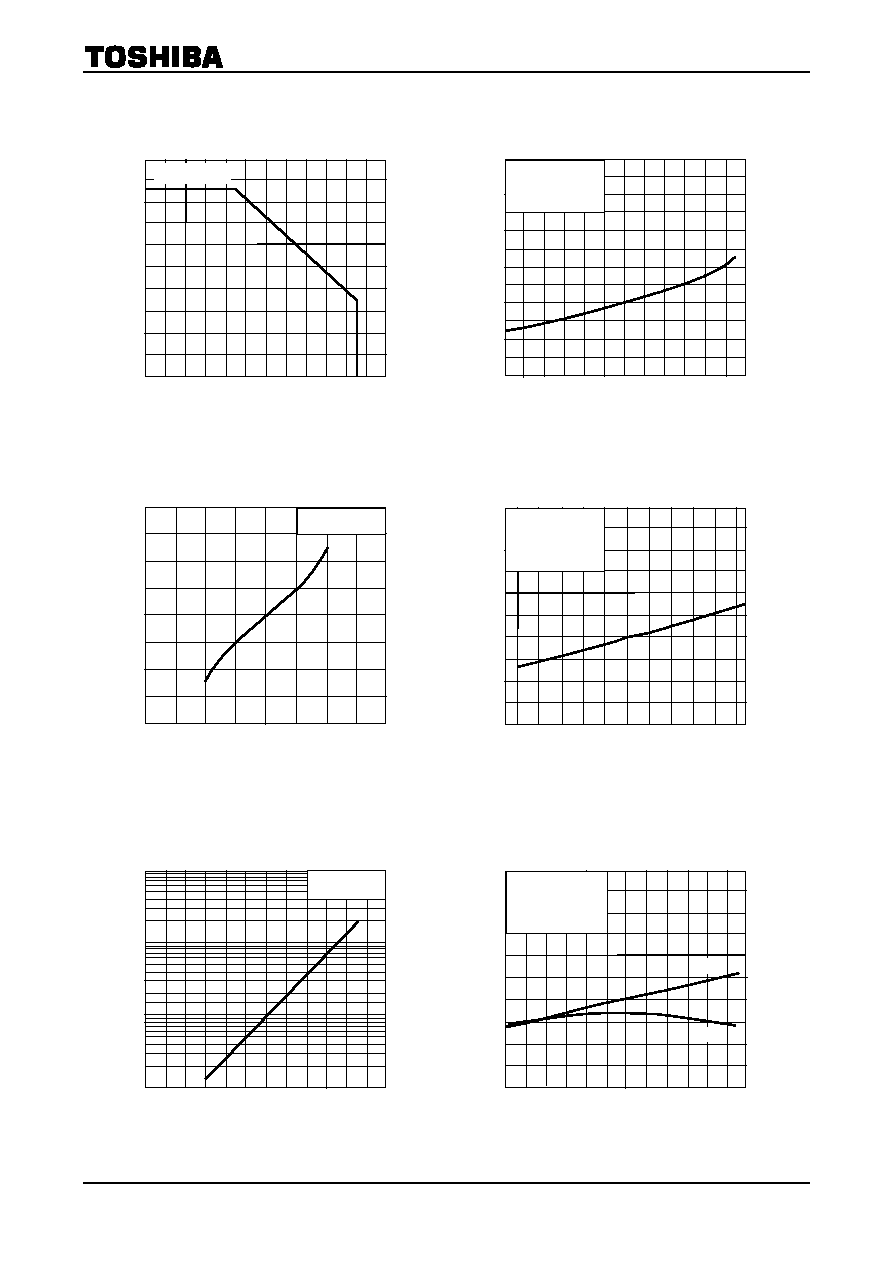
4
I
ON
(RMS) T
a
Amebient temperature Ta (°C)
On-s
t
a
t
e
c
u
r
r
en
t I
ON
(R
MS
)
(mA
)
I
F
V
F
Forward voltage V
F
(V)
Fo
rw
ar
d
c
u
r
r
en
t I
F
(m
A
)
100
0.1
0.6
50
30
10
5
3
1
0.5
0.3
0.8 1.0 1.2 1.4 1.6 1.8
Ta = 25 °C
I
FP
V
FP
Pulse forward voltage V
FP
(V)
P
u
l
s
e
f
o
rward
c
u
rrent
I
FP
(m
A
)
1000
1
0.6
500
300
100
50
30
10
5
3
1.0 1.4 1.8 2.2 2.6 3.0
Pulse width 10 µs
Repetitive frequency = 100 Hz
Ta = 25 °C
V
F
/Ta I
F
Forward current I
F
(mA)
Forward v
o
l
t
age
t
e
m
perat
ure
c
oef
f
i
c
i
ent
V
F
/
T
a
(m
A
/
°
C
)
2.8
0.4
0.3
50
0.1
0.8
1.2
1.6
2.0
2.4
0.5 1
3 5 10
30
I
FP
D
R
Duty cycle ratio D
R
A
l
l
o
w
abl
e p
u
l
s
e
fo
rw
a
r
d c
u
r
r
e
n
t
I
FP
(
m
A
)
5000
10
3000
1000
500
300
100
50
30
10
3
3 10
2
3 10
1
3 10
0
Pulse width 100 µs
Ta = 25 °C
I
F
T
a
Ambient temperature Ta (°C)
A
l
l
o
w
abl
e fo
rw
a
r
d
cu
rre
nt
I
F
(
m
A
)
100
0
20
80
60
40
20
0 20 40 60 80 100
120
C connection
300
0
20
250
200
150
50
0 20 40 60 80 100
100
B connection
A connection
TLP599G
2002-09-25
5
I
FT
T
a
Amebient temperature Ta (°C)
Re
la
tiv
e
t
r
ig
g
e
r
L
E
D c
u
r
r
e
n
t
I
FT
/ I
FT
(
T
a
=
25
°C
)
3.0
0
20
2.5
2.0
1.5
0.5
0 20 40 60 80
1.0
ION = rated
A connection
I
ON
V
ON
(A connection)
On-state current VON (V)
On-s
t
a
t
e
c
u
r
r
en
t I
ON
(
m
A
)
200
200
4
100
0
100
2 0 2 4
Ta = 25 °C
IF = 10 mA
R
ON
T
a
Amebient temperature Ta (°C)
On-
s
t
a
t
e
r
e
sis
t
a
n
ce
R
ON
(R
MS
)
(
)
20
0
20
16
12
8
4
0 20 40 60 80
ION = Rated
IF = 10 mA
tRON < 1 s
A connection
I
OFF
T
a
Ambient temperature Ta (°C)
Of
f-s
t
at
e
c
u
r
r
en
t I
OFF
(
n
A
)
1000
1
20
500
300
100
50
30
10
5
3
0 20 40 60 80
100
VOFF = 400 V
t
ON,
t
OFF
T
a
Ambient temperature Ta (°C)
Switch
in
g
ti
m
e
t
ON,
t
OFF
(
µ
s)
500
0
20
400
300
200
100
0 20 40 60 80
IF = 7.5 mA
R
L
= 200
V
DD
= 20 V
t
OFF
t
ON
P
c
T
a
Ambient temperature Ta (°C)
A
l
l
o
w
abl
e
M
O
S
F
E
T
pow
er di
ssi
pati
o
n
P
c (
m
W
)
500
0
20
400
300
200
100
0 20 40 60 80 100
A connection