 | –≠–ª–µ–∫—Ç—Ä–æ–Ω–Ω—ã–π –∫–æ–º–ø–æ–Ω–µ–Ω—Ç: TLP628 | –°–∫–∞—á–∞—Ç—å:  PDF PDF  ZIP ZIP |

TLP628,TLP628
-2,TLP628-4
2002-09-25
1
TOSHIBA Photocoupler GaAs Ired & Photo-Transistor
TLP628,TLP628-2,TLP628-4
Programmable Controllers
DC-Output Module
Telecommunication
The TOSHIBA TLP628, -2, and -4 consists of a gallium arsenide
infreared emitting diode optically coupled to a phototransistor which
has a 350V high voltage of collector-emitter breakdown voltage.
The TLP628-2 offers two isolated channels in a eight lead plastic
DIP package, while the TLP628-4 provide four isolated channels per
package.
∑ Collector-emitter voltage: 350 V (min.)
∑ Current transfer ratio: 50% (min.)
∑ Isoration voltage: 5000Vrms (min.)
∑ UL recognized: UL1577, file No. E67349
Pin Configurations
(top view)
TLP628
1
2
4
3
1: Anode
2: Cathode
3: Emitter
4: Collector
TLP628-2
1
2
4
3
5
6
7
8
1, 3: Anode
2, 4: Cathode
5, 7: Emitter
6, 8: Collector
TLP628-4
1
2
4
3
5
6
7
8
9
10
11
12
13
14
15
16
1, 3, 5, 7: Anode
2, 4, 6, 8: Cathode
9, 11, 13, 15: Emitter
10, 12, 14, 16: Collector
TOSHIBA 11-5B2
Weight: 0.26g
TOSHIBA 11-10C4
Weight: 0.54g
TOSHIBA 11-20A3
Weight: 1.1g
Unit in mm

TLP628,TLP628
-2,TLP628-4
2002-09-25
2
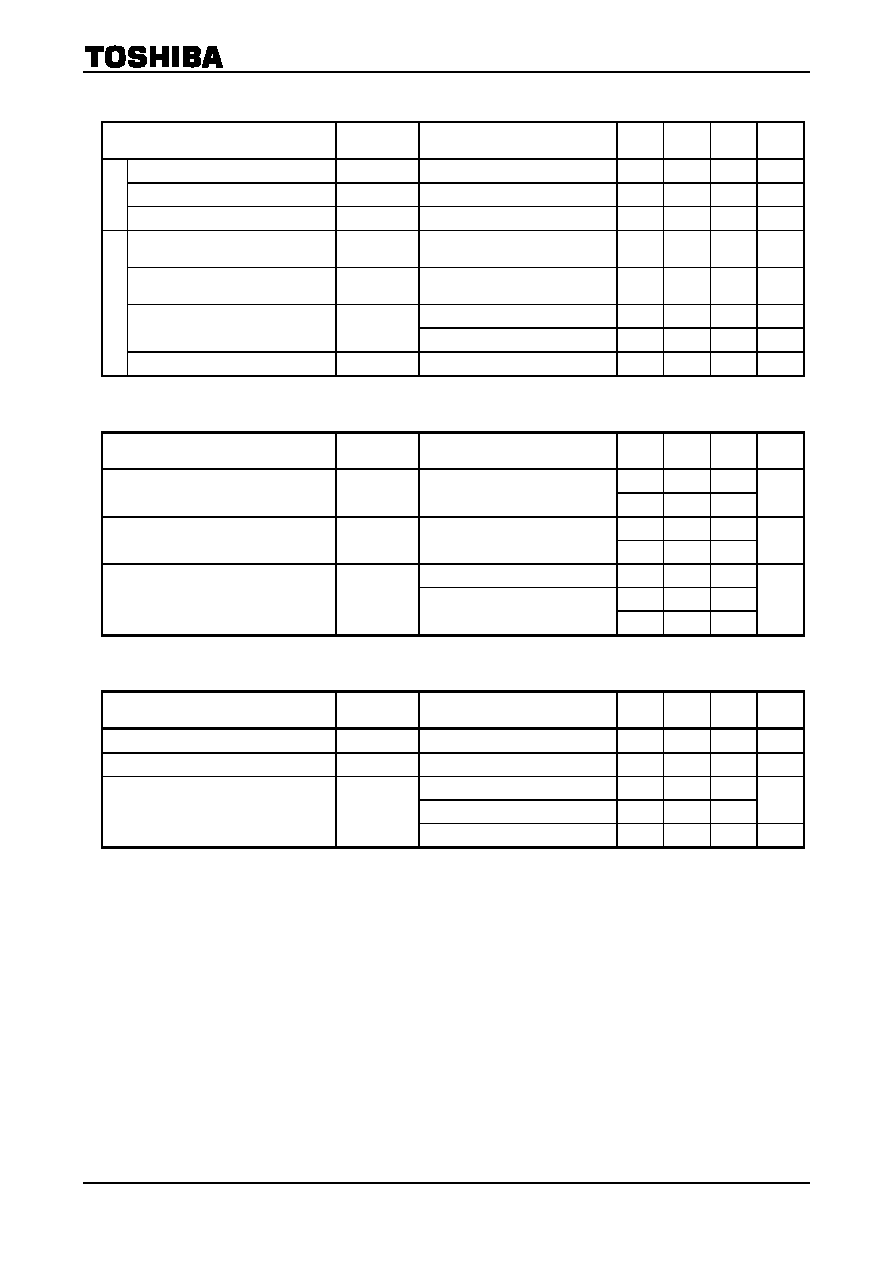
Maximum Ratings
(Ta = 25∞C)
Rating
Charactoristic Symbol
TLP628
TLP628
-2
TLP628
-4
Unit
Forward current
I
F
60 50
mA
Forward current derating
I
F
/ ∞C
-0.7 (Ta 39∞C) -0.5 (Ta 25∞C) mA / ∞C
Pulse forward current
I
FP
1 (100µs pulse, 100pps)
A
Reverse voltage
V
R
5
V
LE
D
Junction temperature
T
j
125
∞C
Collector
-emitter voltage
V
CEO
350 V
Emitter
-collector valtage
V
ECO
7 V
Collector current
I
C
50
mA
Collector power dissipation (1 circuit)
P
C
150 100
mW
Collector power dissipation derating
(Ta 25∞C, 1 circuit)
P
C
/ ∞C
-1.5
-1.0 mW
/
∞C
Det
e
c
t
or
Junction temperature
T
j
125
∞C
Storage temperature range
T
stg
-55~125 ∞C
Operating temperature range
T
opr
-55~100 ∞C
Lead soldering temperature
T
sol
260
(10s)
∞C
Total package power dissipation (1 circuit)
P
T
200 150
mW
Total package power dissipation derating
(Ta 25∞C, 1 circuit)
P
T
/ ∞C
-2.0
-1.5 mW
/
∞C
Isolation voltage
BV
S
5000 (AC, 1min., R.H. 60%)
(Note 1)
Vrms
(Note 1) Device considered a two terminal device: LED side pins shorted together and
detector side pins shorted together.
Recommended Operating Conditions
Characterictic Symbol
Min.
Typ.
Max.
Unit
Supply voltage
V
CC
200
V
Forward current
I
F
16 25 mA
Collector current
I
C
10 mA
Operating temperature
T
opr
-25
85 ∞C
TLP628,TLP628
-2,TLP628-4
2002-09-25
3
Individual Electrical Characteristics
(Ta = 25∞C)
Characteristic Symbol
Test
Condition
Min.
Typ.
Max.
Unit
Forward voltage
V
F
I
F
= 10 mA
1.0
1.15
1.3
V
Reverse current
I
R
V
R
= 5 V
10 µA
LE
D
Capacitance C
T
V = 0, f = 1 MHz
30 pF
Collector
-emitter
breakdown voltage
V
(BR) CEO
I
C
= 0.1 mA
350
V
Emitter
-collector
breakdown voltage
V
(BR) ECO
I
E
= 0.1 mA
7
V
V
CE
= 300 V
10 200
nA
Collector dark current
I
CEO
V
CE
= 300 V, Ta = 85∞C
50 µA
Det
e
c
t
or
Capacitance collector to emitter
C
CE
V = 0, f = 1 MHz
10 pF
Coupled Electrical Characteristics
(Ta = 25∞C)
Characteristic Symbol
Test
Condition
Min.
Typ.
Max.
Unit
50
600
Current transfer ratio
I
C
/ I
F
I
F
= 5 mA, V
CE
= 5 V
Rank GB
100
600
%
60
Saturated CTR
I
C
/ I
F (sat)
IF = 1 mA, V
CE
= 0.4 V
Rank GB
30
%
I
C
= 2.4 mA, I
F
= 8 mA
0.4
0.2
Collector
-emitter
saturation voltage
V
CE (sat)
I
C
= 0.2 mA, I
F
= 1 mA
Rank GB
0.4
V
Isolation Characteristics
(Ta = 25∞C)
Characteristic Symbol
Test
Condition
Min.
Typ.
Max.
Unit
Capacitance input to output
C
S
V
S
= 0, f = 1 MHz
0.8 pF
Isolation resistance
R
S
V
S
= 500 V R.H. 60%
5◊10
10
10
14
AC, 1 minute
5000
AC, 1 second, in oil
10000
V
rms
Isolation voltage
BV
S
DC, 1 minute, in oil
10000
V
dc

TLP628,TLP628
-2,TLP628-4
2002-09-25
4
Switching Characteristics
(Ta = 25∞C)
Characteristic Symbol
Test
Condition
Min.
Typ.
Max.
Unit
Rise time
t
r
2
Fall time
t
f
3
Turn
-on time
t
on
3
Turn
-off time
t
off
V
CC
= 10 V, I
C
= 2 mA
AR
L
= 100
3
µs
Turn
-on time
t
ON
3
Storage time
t
s
40
Turn
-off time
t
OFF
R
L
= 1.9 k (Fig.1)
V
CC
= 5 V, I
F
= 16 mA
90
µs
Fig. 1 Switching time test circuit
I
F
R
L
V
CC
V
CE
V
CE
t
ON
I
F
t
OFF
V
CC
4.5V
0.5V
t
S

TLP628,TLP628
-2,TLP628-4
2002-09-25
5
I
F
≠ V
F
Forward voltage V
F
(V)
Fo
rw
ar
d
c
u
r
r
en
t I
F
(m
A
)
100
0.1
0.4
50
30
3
1
0.3
0.6 0.8 1.0 1.2 1.4 1.6
0.5
5
10
Ta = 25∞C
I
FP
≠ D
R
Duty cycle ratio D
R
A
l
l
o
w
abl
e p
u
l
s
e
fo
rw
a
r
d c
u
r
r
e
n
t
I
FP
(
m
A
)
5000
10
10
-3
1000
500
300
100
50
30
10
-2
10
-1
10
3 3 3 3
3000
Pulse width 100µs
Ta = 25∞C
I
F
≠ Ta
Ambient temperature Ta (∞C)
A
l
l
o
w
abl
e fo
rw
a
r
d
cu
rre
nt
I F
(mA
)
0
100
-20
80
60
40
20
0 20 40 60 80
120
100
TLP628.
TLP628-2,-4
P
C
≠ Ta
Ambient temperature Ta (∞C)
A
l
l
o
w
abl
e col
l
ect
o
r
pow
er
di
ssi
pati
o
n P
C
(m
W
)
200
0
-20
160
120
80
40
0 20 40 60 80
120
100
TLP628.
TLP628-2,-4
I
FP
≠ V
FP
Pulse forward voltage V
FP
(V)
P
u
l
s
e f
o
rw
ar
d cu
rr
ent
I
FP
(m
A
)
0
1000
1
500
300
30
10
3
0.4
0.8 1.2
2.0 2.4
5
50
100
1.6
Pulse width 100µs
Repetitive
Frequency = 100 Hz
Ta = 25∞C
V
F
/Ta ≠ I
F
Forward current I
F
(mA)
Fo
rw
ar
d v
o
l
t
age
te
mp
er
atu
r
e
coefficie
n
t
V
F
/
Ta
(
m
V
/
∞
C
)
5
-0.4
0.1 0.3 1 3
10 30 50
-0.8
-1.2
-1.6
-2.0
-2.4
-2.8
0.5