 | –≠–ª–µ–∫—Ç—Ä–æ–Ω–Ω—ã–π –∫–æ–º–ø–æ–Ω–µ–Ω—Ç: TLP629-2 | –°–∫–∞—á–∞—Ç—å:  PDF PDF  ZIP ZIP |
TLP629,TLP629
-2,TLP629-4
2002-09-25
1
TOSHIBA Photocoupler GaAs Ired & Photo-Transistor
TLP629,TLP629
-
-
-
-
2,TLP629
-
-
-
-
4
Telecommunication
Office Machine
Telephone Use Equipment
The TOSHIBA TLP629, -2, and -4 consists of a photo-transistor
optically coupled to a gallium arsenide infrared emitting diode.
The TLP629-2 offers two isolated channels in an eight lead plastic DIP,
while the TLP629-4 provides four isolated channels in a sixteen plastic
DIP. This is suitable for application of DC input current up to 150mA.
∑ I
F
maximum rating: 150mA
∑ Collector-emitter voltage: 55V (min.)
∑ Current transfer ratio: 25% (min.) (I
F
=20mA)
∑ Isolation voltage: 5000V
rms
(min.)
∑ UL recognized: UL1577, file no. E67349
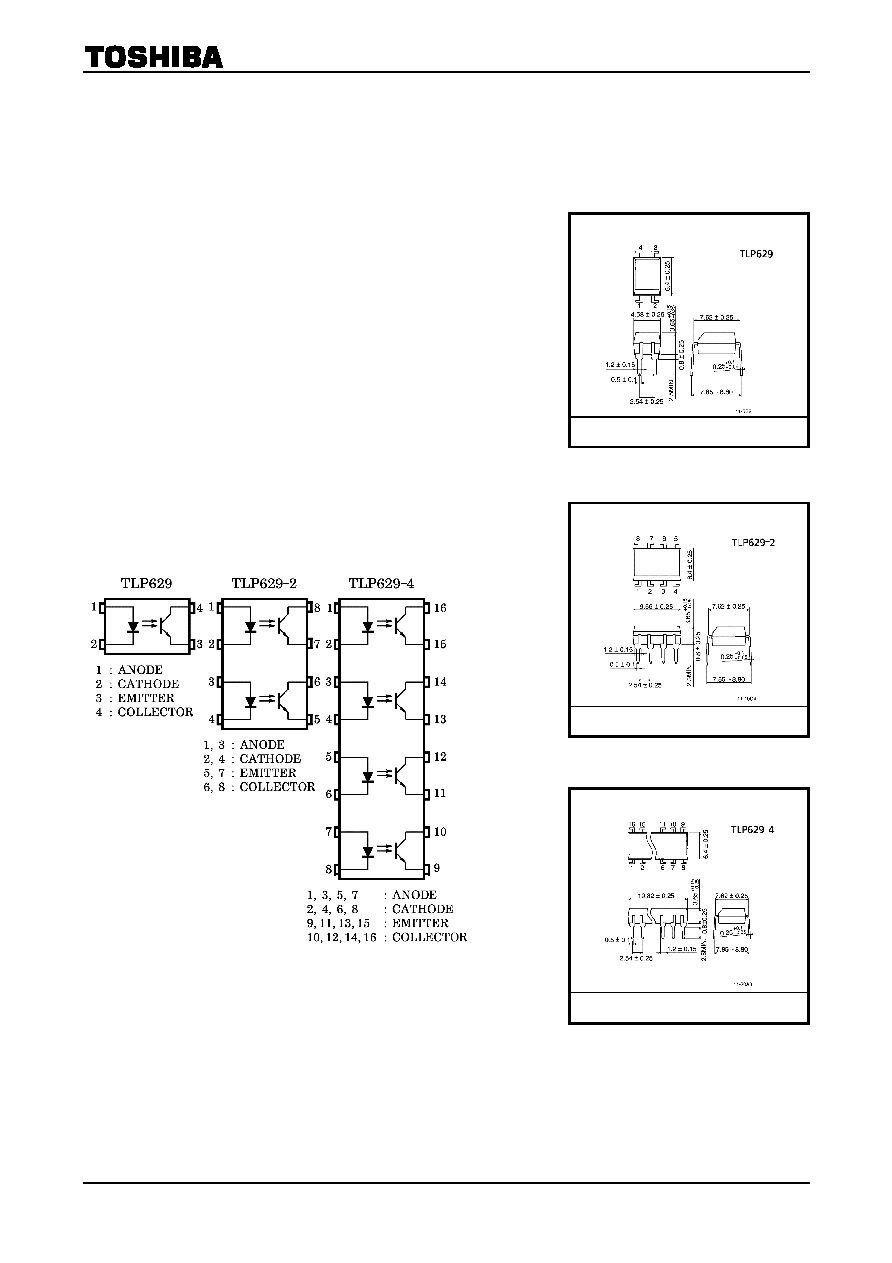
Pin Configurations
(top view)
TOSHIBA 11-5B2
Weight: 0.26 g
TOSHIBA 11-10C4
Weight: 0.54 g
TOSHIBA 11-20A3
Weight: 1.1 g
Unit in mm

TLP629,TLP629
-2,TLP629-4
2002-09-25
2
Maximum Ratings
(Ta = 25∞C)
Rating
Characteristic Symbol
TLP629 TLP629
-2,4
Unit
Forward current
I
F
150
mA
Forward current derating
I
F
/ ∞C
-1.5 (Ta 25∞C)
mA / ∞C
Pulse forward current
I
FP
1 (100µs pulse, 100pps)
A
Reverse voltage
V
R
5 V
LE
D
Junction temperature
T
j
125
∞C
Collector
-emitter voltage
V
CEO
55 V
Emitter
-collector valtage
V
ECO
7 V
Collector current
I
C
80
mA
Collector power dissipation
(1 circuit)
P
C
150 100
mW
Collector power dissipation derating
(1 circuit, Ta 25∞C)
P
C
/ ∞C
-1.5
-1.0 mW
/
∞C
Det
e
c
t
or
Junction temperature
T
j
125
∞C
Storage temperature range
T
stg
-55~125 ∞C
Operating temperature range
T
opr
-55~100 ∞C
Lead soldering temperature
T
sol
260
(10s) ∞C
Total package power dissipation
P
T
250 200
mW
Total package power dissipation derating
(Ta25∞C)
P
T
/ ∞C
-2.5 2.0
mW
/
∞C
Isolation voltage
(Note 1)
BV
S
5000 (AC, 1min., RH 60%)
V
rms
(Note 1) Device considered a two terminal: LED side pins shorted together, and detector
side pins shorted together.
Recommended Operating Conditions
Characteristics Symbol
Min.
Typ.
Max.
Unit
Supply voltage
V
CC
5 24 V
Forward current
I
F
20 120
mA
Collector current
I
C
1 10 mA
Operating temperature
T
opr
-25
85 ∞C

TLP629,TLP629
-2,TLP629-4
2002-09-25
3
Individual Electrical Characteristics
(Ta = 25∞C)
Characteristic Symbol
Test
Condition
Min.
Typ.
Max.
Unit
Forward voltage
V
F
I
F
= 100 mA
--
1.4
1.7
V
Forward current
I
F
V
F
=
0.7
V
-- 2.5 20 µA
Reverse current
I
R
V
R
= 5 V
--
--
10
µA
LE
D
Capacitance C
T
V = 0, f = 1 MHz
--
50
--
pF
Collector
-emitter
breakdown voltage
V
(BR) CEO
I
C
= 0.5 mA
55
--
--
V
Emitter
-collector
breakdown voltage
V
(BR) ECO
I
E
= 0.1 mA
7
--
--
V
V
CE
= 24 V
--
10
100
nA
Collector dark current
I
CEO
V
CE
= 24 V, Ta = 85∞C
--
2
50
µA
Det
e
c
t
or
Capacitance collector to emitter
C
CE
V = 0, f = 1 MHz
--
10
--
pF
Coupled Electrical Characteristics
(Ta = 25∞C)
Characteristic Symbol
Test
Condition
MIn.
Typ.
Max.
Unit
I
C
/ I
F
I
F
= 20 mA, V
CE
= 1 V
25
--
--
Current transfer ratio
I
C
/ I
F
(high)
I
F
= 100 mA, V
CE
= 1 V
20
--
80
%
I
C
= 2.4 mA, I
F
= 20 mA
--
--
0.4
Collector
-emitter saturation voltage
V
CE (sat)
I
C
= 2.4 mA, I
F
= 100 mA
--
--
0.4
V
Off
-state collector current
I
C(off)
V
F
= 0.7V, V
CEO
= 24 V
--
1
1.0
µA
Isolation Characteristics
(Ta = 25∞C)
Characteristic Symbol
Test
Condition
Min.
Typ.
Max.
Unit
Capacitance input to output
C
S
V
S
= 0, f = 1 MHz
--
0.8
--
pF
Isolation resistance
R
S
V
S
= 500 V
5◊10
10
10
14
--
AC, 1 minute
5000
--
--
AC, 1 second, in oil
--
10000
--
V
rms
Isolation voltage
BV
S
DC, 1 minute, in oil
--
10000
--
Vdc

TLP629,TLP629
-2,TLP629-4
2002-09-25
4
Switching Characteristics
(Ta = 25∞C)
Characteristic Symbol
Test
Condition
Min.
Typ.
Max.
Unit
Rise time
t
r
-- 2 --
Fall time
t
f
-- 3 --
Turn
-on time
t
on
-- 3 10
Turn
-off time
t
off
V
CC
= 10 V, I
C
= 2 mA
R
L
= 100
-- 3 10
µs
Turn
-on time
t
ON
-- 2 --
Storage time
t
s
-- 15 --
Turn
-off time
t
OFF
R
L
= 1.9 k (Fig.1)
V
CC
= 5 V, I
F
= 16 mA
-- 25 --
µs
Fig. 1 Switching time test circuit

TLP629,TLP629
-2,TLP629-4
2002-09-25
5