 | –≠–ª–µ–∫—Ç—Ä–æ–Ω–Ω—ã–π –∫–æ–º–ø–æ–Ω–µ–Ω—Ç: TLP759 | –°–∫–∞—á–∞—Ç—å:  PDF PDF  ZIP ZIP |
TLP759(IGM)
2003-02-19
1
TOSHIBA
Photocoupler
GaAAs Ired + Photo IC
TLP759(IGM)
Transistor Invertor
Inverter For Air Conditioner
Line Receiver
IPM Interfaces
The TOSHIBA TLP759(IGM) consists of a GaAAs high
-
output light
emitting diode and a high speed detector of one chip photo diode-
transistor.
This unit is 8
-
lead DIP.
TLP759(IGM) has no internal base connection, and a faraday shield
integrated on the photodetector chip provides an effective common
mode noise transient immunity.
TLP759(IGM) guarantees minimum and maximum of propagation
delay time, switching time dispersion, and high common mode
transient immunity. Therefor TLP759(IGM) is suitable for isolation
interface between IPM(intelligent power module) and control IC
circuits in motor control application.
∑ Isolation voltage: 5000V
rms
(min.)
∑ Common mode transient immunity
: ±10kV / µs (min.)
@V
CM
= 1500 V
∑ Switching Time
: t
pHL,
t
pLH
= 0.1µs (min.)
= 0.8µs (max.)
@I
F
= 10mA,V
CC
= 15V,R
L
= 20k,Ta = 25∞C
∑ Switching time dispersion: 0.7µs (max.)
(|t
pLH
-t
pHL
|)
∑ TTL compatible
∑ UL recognized: UL1577, file no.E67349
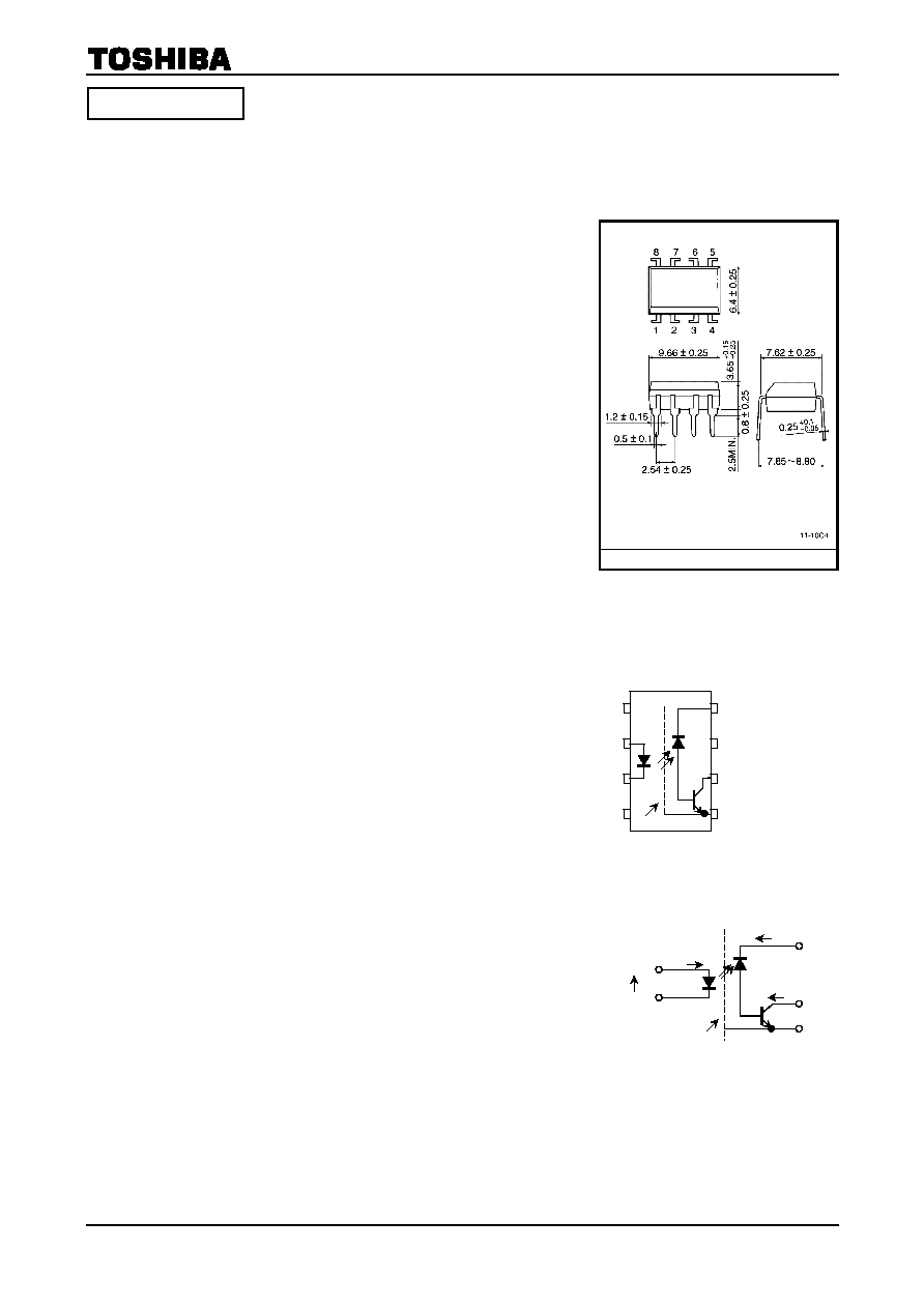
Pin Configuration
(top view)
1 : N.C.
2 : Anode
3 : Cathode
4 : N.C.
5 : Emitter
6 : Collector
7 : N.C.
8 : V
CC
7
8
6
2
1
3
4
5
Shield
Schematic
8
6
2
3
V
O
5
Shield
GND
V
CC
I
O
I
CC
V
F
I
F
TOSHIBA 11
-10C4
Weight: 0.54 g
Unit in mm
TENTATIVE

TLP759(IGM)
2003-02-19
2
∑ Option (D4) type
VDE approved: DIN VDE0884 / 06.92,
Maximum operating insulation voltage: 890V
PK
Highest permissible over voltage: 6000V
PK
(Note 1) When a VDE0884 approved type is needed,
please designate the "Option (D4)"
∑ Structural parameter
7.62mm pich TLP759 (IGM)
Creepage distance: 7.0mm (min.)
Clearance: 7.0mm (min.)
Insulation thickness: 0.4mm (min.)
Maximum Ratings
(Ta = 25∞C)
Characteristic Symbol
Rating
Unit
Forward current
(Note 2)
I
F
25 mA
Pulse forward current
(Note 3)
I
FP
50 mA
Peak transient forward current
(Note 4)
I
FPT
1 A
Reverse voltage
V
R
5 V
LE
D
Diode power dissipation
(Note 5)
P
D
45 mW
Output current
I
O
8 mA
Peak output current
I
OP
16 mA
Output voltage
V
O
-0.5~20 V
supply voltage
V
CC
-0.5~30 V
Det
e
c
t
or
Output power dissipation
(Note 6)
P
O
100 mW
Operating temperature range
T
opr
-55~100
∞C
Storage temperature range
T
stg
-55~125
∞C
Lead solder temperature(10s)
(Note 7)
T
sol
260
∞C
Isolation voltage(AC,1min.,R.H.60%,Ta=25∞C) (Note
8)
BV
S
5000 V
rms
(Note 2): Derate 0.8mA above 70∞C.
(Note 3): 50% duty cycle,1ms pulse width.
Derate 1.6mA / ∞C above 70∞C.
(Note 4): Pulse width PW 1µs,300pps.
(Note 5): Derate 0.9mW / ∞C above 70∞C.
(Note 6): Derate 2mW / ∞C above 70∞C.
(Note 7): Soldering portion of lead: Up to 2mm from the body of the device.
(Note 8): Device considerd a two terminal device: Pins 1, 2, 3 and 4 shorted together and
pins 5, 6, 7 and 8 shorted together.

TLP759(IGM)
2003-02-19
3
Electrical Characteristics
(Ta = 25∞C)
Characteristic Symbol
Test
Condition
Min.
Typ.
Max.
Unit
Forward voltage
V
F
I
F
= 16mA
1.65
1.85
V
Forward voltage
temperature coefficient
V
F
/ Ta I
F
= 16mA
-2
mV / ∞C
Reverse current
I
R
V
R
= 5V
10 µA
LE
D
Capacitance between
terminal
C
T
V
F
= 0,f = 1MHz
45 pF
I
OH (1)
I
F
= 0mA,V
CC
= V
O
= 5.5V
3 500
nA
I
OH (2)
I
F
= 0mA,V
CC
= 30V
V
O
= 20V
5
High level output current
I
OH
I
F
= 0mA,V
CC
= 30V
V
O
= 20V,Ta = 70∞C
50
µA
High level supply
voltage
I
CCH
I
F
= 0mA,V
CC
= 30V
0.01 1 µA
Supply voltage
V
CC
I
CC
= 0.01mA
30
V
Det
e
c
t
or
Output voltage
V
O
I
O
= 0.5mA
20
V
Coupled Electrical Characteristics
(Ta = 25∞C)
Characteristic Symbol
Test
Condition
Min.
Typ.
Max.
Unit
I
F
= 10mA,V
CC
= 4.5V
V
O
= 0.4V
25 35 75
Current transfer ratio
I
O
/ I
F
I
F
= 16mA,V
CC
= 4.5V
V
O
= 0.4V,Ta =
-25~100∞C
15
%
Low level output voltage
V
OL
I
F
= 16mA,V
CC
= 4.5V
I
O
= 2.4mA
0.4 V
Isolation Characteristics
(Ta = 25∞C)
Characteristic Symbol
Test
Condition
Min.
Typ.
Max.
Unit
Capacitance input to output
C
S
V = 0,f = 1MHz
(Note 8)
0.8 pF
Isolation resistance
R
S
R.H. 60%,V
S
= 500V
(Note
8)
1◊10
12
10
14
AC,1 minute
5000
V
rms
AC,1 second,in oil
10000
Isolation voltage
BV
S
DC,1 minute,in oil
10000
Vdc

TLP759(IGM)
2003-02-19
4
Switching Characteristics
(Ta = 25∞C,V
CC
= 15V)
Characteristic Symbol
Test
Cir
-
cuit
Test Condition
Min.
Typ.
Max.
Unit
I
F
= 10mA,R
L
= 20k 0.1
0.45
0.8
I
F
= 10mA,R
L
= 20k
Ta = 0~85∞C
0.1 0.45 0.9
Propagation delay time
(HL)
Propagation delay time
(LH)
t
pHL
t
pLH
I
F
= 10mA,R
L
= 20k
Ta =
-25~100∞C
0.1 0.45 1.0
µs
I
F
= 10mA,R
L
= 20k
0.15 0.7
I
F
= 10mA,R
L
= 20k
Ta = 0~85∞C
0.25 0.8
Switching time
dispersion between on
and off
|t
pLH
-t
pHL
|
1
I
F
= 10mA,R
L
= 20k
Ta =
-25~100∞C
0.25 0.9
µs
Common mode
transient immunity at
logic high output
(Note
9)
CM
H
I
F
= 0mA
V
CM
= 1500V
p
-p
R
L
= 20k
10000 15000 V
/
µs
Common mode
transient immunity at
logic low output
(Note
9)
CM
L
2
I
F
=10mA
V
CM
= 1500V
p
-p
R
L
= 20k
-10000 -15000
V
/
µs
(Note 9): CM
L
is the maximum rate of fall of the common mode voltage that can be
sustained with the output voltage in the logic low state(V
O
< 1V).
CM
H
is the maximum rate of rise of the common mode voltage that can be
sustained with the output voltage in the logic high state(V
O
< 4V).
(Note 10): Maximum electrostatic discharge voltage for any pins: 100V(C = 200pF, R = 0).
Test Circuit 1: Switching Time Test Circuit
t
p
HL
15V
V
O
I
F
1.5V
1.5V
V
OL
0
t
pLH
I
F
1
51
2
3
4
8
7
6
5
PW = 100µs
Duty ratio = 1 / 10
V
CC
= 15 V
R
L
V
O
Output
monitor
Pulse input
I
F
Monitor
0.
1µ
F

TLP759(IGM)
2003-02-19
5
Test Circuit 2: Common Mode Noise Immunity Test Circuit
s)
(
f
t
1200(V)
L
CM
s)
(
r
t
1200(V)
H
CM
m
=
,
m
=
V
O
(I
F
= 0mA)
V
O
Output
monitor
V
O
(I
F
= 10mA)
t
r
V
CM
15V
90%
1500V
0V
t
f
10%
4V
1V
V
OL
V
CM
I
F
1
2
3
4
8
7
6
5
V
CC
= 15 V
R
L
Pulse generator
Z
O
= 50
0.
1µ
F