 | –≠–ª–µ–∫—Ç—Ä–æ–Ω–Ω—ã–π –∫–æ–º–ø–æ–Ω–µ–Ω—Ç: TPC6101 | –°–∫–∞—á–∞—Ç—å:  PDF PDF  ZIP ZIP |
TPC6101
2002-01-17
1
TOSHIBA Field Effect Transistor Silicon P Channel MOS Type (U-MOSII)
TPC6101
Notebook PC Applications
Portable Equipment Applications
∑ Low drain-source ON resistance: R
DS (ON)
= 48 m (typ.)
∑ High forward transfer admittance: |Y
fs
| = 8.2 S (typ.)
∑ Low leakage current: I
DSS
= -10 µA (max) (V
DS
= -20 V)
∑ Enhancement-model: V
th
= -0.5 to -1.2 V (V
DS
= -10 V,
I
D
= -200 µA)
Maximum Ratings
(Ta
=
=
=
=
25∞C)
Characteristics Symbol
Rating
Unit
Drain-source voltage
V
DSS
-20 V
Drain-gate voltage (R
GS
= 20 kW) V
DGR
-20 V
Gate-source voltage
V
GSS
±12 V
DC
(Note 1)
I
D
-4.5
Drain current
Pulse
(Note 1)
I
DP
-18
A
Drain power dissipation
(t
= 5 s)
(Note 2a)
P
D
2.2
W
Drain power dissipation
(t
= 5 s)
(Note 2b)
P
D
0.7
W
Single pulse avalanche energy (Note 3)
E
AS
3.3
mJ
Avalanche current
I
AR
-2.25 A
Repetitive avalanche energy (Note 4)
E
AR
0.22 mJ
Channel temperature
T
ch
150
∞C
Storage temperature range
T
stg
-55 to 150
∞C
Thermal Characteristics
Characteristics Symbol
Max
Unit
Thermal resistance, channel to ambient
(t
= 5 s)
(Note 2a)
R
th (ch-a)
56.8
∞C/W
Thermal resistance, channel to ambient
(t
= 5 s)
(Note 2b)
R
th (ch-a)
178.5
∞C/W
Note: (Note 1), (Note 2), (Note 3), (Note 4), (Note 5) Please see next
page.
This transistor is an electrostatically sensitive device. Please handle it
with caution.
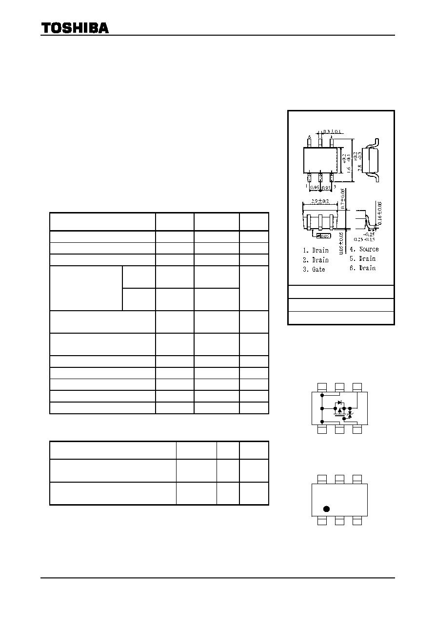
Unit: mm
JEDEC
JEITA
TOSHIBA 2-3T1A
Weight: 0.011 g (typ.)
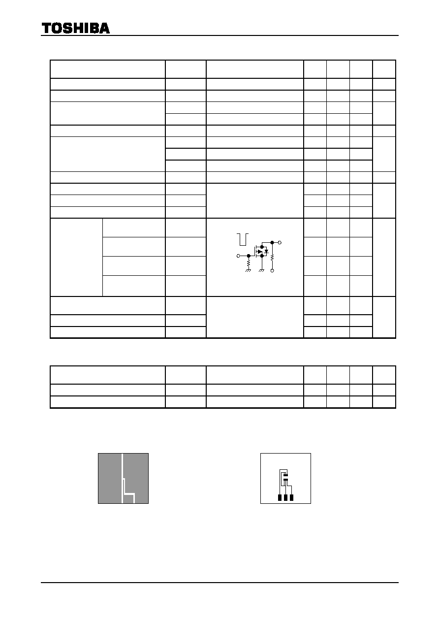
Circuit Configuration
6 4
1 2 3
5
Marking
(Note 5)
S 3 A
TPC6101
2002-01-17
2
Electrical Characteristics
(Ta
=
=
=
=
25∞C)
Characteristics Symbol
Test
Condition
Min
Typ.
Max
Unit
Gate leakage current
I
GSS
V
GS
= ±10 V, V
DS
= 0 V
æ
æ
±10
mA
Drain cut-OFF current
I
DSS
V
DS
= -20 V, V
GS
= 0 V
æ
æ
-10
mA
V
(BR) DSS
I
D
= -10 mA, V
GS
= 0 V
-20
æ
æ
Drain-source breakdown voltage
V
(BR) DSX
I
D
= -10 mA, V
GS
= 12 V
-8
æ
æ
V
Gate threshold voltage
V
th
V
DS
= -10 V, I
D
= -200 mA
-0.5
æ
-1.2
V
R
DS (ON)
V
GS
= -2 V, I
D
= -2.2 A
æ 110 180
R
DS (ON)
V
GS
= -2.5 V, I
D
= -2.2 A
æ 75 100
Drain-source ON resistance
R
DS (ON)
V
GS
= -4.5 V, I
D
= -2.2 A
æ 48 60
m
W
Forward transfer admittance
|Y
fs
| V
DS
= -10 V, I
D
= -2.2 A
4.1 8.2
æ S
Input capacitance
C
iss
æ 830 æ
Reverse transfer capacitance
C
rss
æ 300 æ
Output capacitance
C
oss
V
DS
= -10 V, V
GS
= 0 V, f = 1 MHz
æ 370 æ
pF
Rise time
t
r
æ 6 æ
Turn-ON time
t
on
æ 11 æ
Fall time
t
f
æ 57 æ
Switching time
Turn-OFF time
t
off
Duty <= 1%, t
w
= 10 ms
æ 112 æ
ns
Total gate charge
(gate-source plus gate-drain)
Q
g
æ 12 æ
Gate-source charge
Q
gs
æ 6 æ
Gate-drain ("miller") charge
Q
gd
V
DD
~
- -16 V, V
GS
= -5 V,
I
D
= -4.5 A
æ 6 æ
nC
Source-Drain Ratings and Characteristics
(Ta
=
=
=
=
25∞C)
Characteristics Symbol
Test
Condition
Min
Typ.
Max
Unit
Pulse drain reverse current
(Note 1)
I
DRP
æ
æ
æ
-18
A
Forward voltage (diode)
V
DSF
I
DR
= -4.5 A, V
GS
= 0 V
æ
æ 1.2 V
Note 1: Please use devices on condition that the channel temperature is below 150∞C.
Note 2: (a) Device mounted on a glass-epoxy board (a) (t
= 5 s)
(b) Device mounted on a glass-epoxy board (b) (t
= 5 s)
Note 3: V
DD
= 16 V, T
ch
= 25∞C (initial), L = 0.5 mH, R
G
= 25 W, I
AR
= -2.25 A
Note 4: Repetitive rating; pulse width limited by maximum channel temperature
Note 5: Black round marking
"∑" locates on the left lower side of parts number marking "S3A" indicates terminal
No.1.
(a)
FR-4
25.4
¥ 25.4 ¥ 0.8
Unit:
(mm)
(b)
FR-4
25.4
¥ 25.4 ¥ 0.8
Unit:
(mm)
R
L
=
4.
5
W
V
DD
~
- -10 V
-5 V
V
GS
0 V
4.
7
W
I
D
= -2.2 A
V
OUT

TPC6101
2002-01-17
3
Fo
rw
ar
d
t
r
a
n
sfe
r
ad
mi
ttanc
e |Y
fs
|
(S
)
D
r
ai
n
-
so
urc
e
v
o
l
t
a
ge
V
DS
(V
)
Drain-source voltage V
DS
(V)
I
D
≠ V
DS
D
r
ai
n
cu
rre
nt
I
D
(A
)
Drain-source voltage V
DS
(V)
I
D
≠ V
DS
D
r
ai
n
cu
rre
nt
I
D
(A
)
Gate-source voltage V
GS
(V)
I
D
≠ V
GS
D
r
ai
n
cu
rre
nt
I
D
(A
)
Gate-source voltage V
GS
(V)
V
DS
≠ V
GS
Drain current I
D
(A)
|Y
fs
| ≠ I
D
Drain current I
D
(A)
D
r
ai
n
-
so
urc
e
on resi
s
t
a
n
ce
R
DS
(ON)
(m
9
)
R
DS (ON)
≠ I
D
0
0
-1
-2
-3
-4
-5
-0.4
-0.8
-1.2
-2.0
Common source
Ta
= 25∞C Pulse test
VGS = -1.4 V
-1.6 V
-1.7 V
-1.8 V
-2.0 V
-4 V
-5 V
-3 V
-2.5 V
-1.6
-1.9 V
-5 V
0
-1
-2
-3
-4
-5
-2.0 V
-1.8 V
-2.5 V
-1.6 V
VGS = -1.4 V
-2.2 V
-2.4 V
-3 V
0
-2
-4
-6
-8
-10
Common source
Ta
= 25∞C Pulse test
-4 V
10
1000
-0.1
-1
-10
-100
100
-2.5 V
VGS = -4.5 V
-2.0 V
Common source
Ta
= 25∞C
Pulse test
30
300
-0.3
-3
-30
0
-0.2
-0.4
-0.6
-0.8
-1
0
-2
-4
-6
-8
-10
-1.1 A
-2.2 A
Common source
Ta
= 25∞C
Pulse test
ID = -4.5 A
0.1
1
10
100
-0.1
-1
-10
-100
100∞C
25∞C
Ta
= -55∞C
Common source
VDS = -10 V
Pulse test
0.3
3
30
-0.3
-3
-30
Ta
= -55∞C
0
-2
-4
-6
-8
-10
0
-0.5
-1
-1.5
-2
-2.5
100∞C
25∞C
Common source
VDS = -10 V
Pulse test

TPC6101
2002-01-17
4
Ambient temperature Ta (
∞
C)
R
DS (ON)
≠ Ta
D
r
ai
n
-
so
urc
e
on resi
s
t
a
n
ce
R
DS
(ON)
(m
9
)
Drain-source voltage V
DS
(V)
I
DR
≠ V
DS
D
r
ai
n
re
ver
s
e c
u
r
r
e
n
t
I
DR
(A
)
Drain-source voltage V
DS
(V)
Capacitance ≠ V
DS
C
apaci
t
anc
e C
(p
F)
Ambient temperature Ta (
∞
C)
V
th
≠ Ta
Gate
th
res
hol
d vol
t
a
ge
V
th
(V
)
Ambient temperature Ta (
∞
C)
P
D
≠ Ta
D
r
ai
n
po
w
e
r
di
ssi
p
a
ti
on
P
D
(W
)
Gate
-so
u
r
c
e
v
o
l
t
age
V
GS
(V
)
Total gate charge Q
g
(nC)
Dynamic input/output characteristics
D
r
ai
n
-
so
urc
e
v
o
l
t
a
ge
V
DS
(V
)
-80
-40
0
40
80 160
120
0
-0.8
-1.2
-2.0
Common source
VDS = -10 V
ID = -200 mA
Pulse test
-1.6
-0.4
-1
-10
0 0.4
0.6
0.8
1
1.2
0.2
-100
Common source
Ta
= 25∞C
Pulse test
-2 V
-1 V
VGS = -0 V
-4 V
-3
-30
10
100
1000
10000
-0.1
-1
-10
-100
Crss
Coss
Ciss
Ta
= 25∞C
f
= 1 MHz
VGS = 0 V
-0.3
-3
-30
30
300
3000
0
-4
-8
-10
-6
-2
0
0
-4
4
6
8
10
-8
-12
-20
Common source
ID = -6 A
Ta
= 25∞C
Pulse test
VGS
VDD = -16 V
12 16
18
-16
VDS
-8 V
14
2
0
40
80
100
140
180
-80
-40 0 40
80
160
Common source
Pulse test
120
VGS = -2.0 V
ID = -2.2 A
160
120
60
20
-1.1 A
-4.5 A
-1.1 A
-1.1 A
-2.2 A
-4.5 V
-2.5 V
-4.5 A
-2.2 A
0
0
0.5
1
1.5
2
2.5
40 80
120
160
(1) t
= 5 s
(2) t
= 5 s
(1) DC
(2) DC
(1) Device mounted on a
glass-epoxy board (a)
(Note 2a)
(2) Device mounted on a
glass-epoxy board (b)
(Note 2b)

TPC6101
2002-01-17
5
Safe operating area
Drain-source voltage V
DS
(V)
D
r
ai
n
cu
rre
nt
I
D
(A
)
r
th
- t
w
Pulse t
w
(s)
T
r
a
n
si
e
n
t t
h
e
r
m
a
l
i
m
pe
da
nce
r
th
(∞C
/
W
)
0.1
0.001 0.01 0.1
10
100
1000
1
0.3
3
30
100
300
1000
Single pulse
Device mounted on a glass-
epoxy board (b) (Note 2b)
1
Device mounted on a glass-
epoxy board (a) (Note 2a)
10
-0.001
-0.01 -0.03 -0.1 -0.3
-1
-3
-10
-100
-30
-0.003
-0.01
-0.03
-0.1
-0.3
-10
-1
-3
-100
-30
*: Single pulse Ta
= 25∞C
Curves must be derated
linearly with increase in
temperature
ID max (pulse)*
10 ms*
1 ms*
VDSS
max