 | –≠–ª–µ–∫—Ç—Ä–æ–Ω–Ω—ã–π –∫–æ–º–ø–æ–Ω–µ–Ω—Ç: TPC8302 | –°–∫–∞—á–∞—Ç—å:  PDF PDF  ZIP ZIP |

TPC8302
2002-05-17
1
TOSHIBA Field Effect Transistor Silicon P Channel MOS Type (L
2
--MOSVI)
TPC8302
Lithium Ion Battery Applications
Portable Equipment Applications
Notebook PCs
2.5 V Gate drive
Small footprint due to small and thin package
Low drain-source ON resistance: R
DS
(ON)
= 100 m (typ.)
High forward transfer admittance: |Y
fs
| = 5 S (typ.)
Low leakage current: I
DSS
= -10 µA (max) (V
DS
= -20 V)
Enhancement-mode: V
th
= -0.5~ -1.1 V (V
DS
= -10 V, I
D
= -200 µA)
Maximum Ratings
(Ta = 25∞C)
Characteristics Symbol
Rating
Unit
Drain-source voltage
V
DSS
-20 V
Drain-gate voltage (R
GS
= 20 k)
V
DGR
-20 V
Gate-source voltage
V
GSS
±12 V
D C
(Note 1)
I
D
-3.5
Drain current
Pulse (Note
1) I
DP
-14
A
Single-device
operation (Note 3a)
P
D (1)
1.5
Drain power
dissipation
(t = 10s)
(Note
2a)
Single-devece value
at dual operation
(Note
3b)
P
D (2)
1.0
W
Single-device
operation (Note 3a)
P
D (1)
0.75
Drain power
dissipation
(t = 10s)
(Note
2b)
Single-devece value
at dual operation
(Note
3b)
P
D 2)
0.45
W
Single pulse avalanche energy
(Note
4)
E
AS
16 mJ
Avalanche current
I
AR
-3.5 A
Repetitive avalanche energy
(Note 2a, Note 3b, Note 5)
E
AR
0.1 mJ
Channel temperature
T
ch
150
Storage temperature range
T
stg
-55150
Note: For (Note 1), (Note 2a), (Note 2b), (Note 3a), (Note 3b), (Note 4)
and (Note 5), please refer to the next page.
This transistor is an electrostatic sensitive device. Please handle with caution.
Unit: mm
JEDEC
JEITA
TOSHIBA 2-6J1E
Weight: 0.080 g (typ.)
Circuit Configuration

TPC8302
2002-05-17
2
Thermal Characteristics
Characteristics Symbol
Max
Unit
Single-device operation
(Note 3a)
R
th (ch-a) (1)
83.3
Thermal resistance, channel to ambient
(t = 10s)
(Note 2a) Single-device value at
dual operation
(Note 3b)
R
th (ch-a) (2)
125
Single-device operation
(Note 2a)
R
th (ch-a) (1)
167
Thermal resistance, channel to ambient
(t = 10s)
(Note 2b) Single-device value at
dual operation
(Note 2b)
R
th (ch-a) (2)
278
∞C/W
Marking
Note 1: Please use devices on condition that the channel temperature is below 150∞C.
Note 2:
a) Device mounted on a glass-epoxy board (a)
b) Device mounted on a glass-epoxy board (b)
Note 3:
a) The power dissipation and thermal resistance values are shown for a single device
(During single-device operation, power is only applied to one device.)
b) The power dissipation and thermal resistance values are shown for a single device
(During dual operation, power is evenly applied to both devices.)
Note 4:
V
DD
= -16 V, T
ch
= 25∞C (Initial), L = 1.0 mH, R
G
= 25 , I
AR
= -3.5 A
Note 5: Repetitive rating: pulse width limited by maximum channel temperature
Note 6:
∑
on lower left of the marking indicates Pin 1.
* shows lot number. (year of manufacture: last decimal digit of the year of manufacture, month of
manufacture: January to December are denoted by letters A to L respectively.)
*
Type
TPC8302
FR-4
25.4
◊
25.4
◊
0.8
(unit: mm)
(a)
FR-4
25.4
◊
25.4
◊
0.8
(unit: mm)
(b)

TPC8302
2002-05-17
3
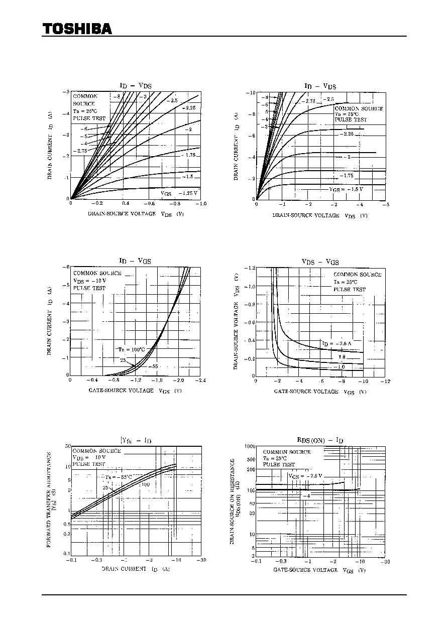
Electrical Characteristics
(Ta = 25∞C)
Characteristics Symbol
Test
Condition
Min
Typ.
Max
Unit
Gate leakage current
I
GSS
V
GS
= ±10 V, V
DS
= 0 V
-- -- ±10 µA
Drain cut-OFF current
I
DSS
V
DS
= -20 V, V
GS
= 0 V
-- -- -10 µA
Drain-source breakdown voltage
V
(BR) DSS
I
D
= -10 mA, V
GS
= 0 V
-20 -- -- V
Gate threshold voltage
V
th
V
DS
= -10 V, I
D
= -200 µA
-0.5 -- -1.1 V
R
DS (ON)
V
GS
= -2.5 V, I
D
= -1.8 A
-- 135 170
Drain-source ON resistance
R
DS (ON)
V
GS
= -4 V, I
D
= -1.8 A
-- 100 120
m
Forward transfer admittance
|Y
fs
| V
DS
= -10 V, I
D
= -1.8 A
2.5 5 -- S
Input capacitance
C
iss
-- 680 --
Reverse transfer capacitance
C
rss
--
90
--
Output capacitance
C
oss
V
DS
= -10 V, V
GS
= 0 V, f = 1 MHz
-- 310 --
pF
Rise time
t
r
--
17
--
Turn-ON time
t
on
--
24
--
Fall time
t
f
--
20
--
Switching time
Turn-OFF time
t
off
-- 63 --
ns
Total gate charge (Gate-source
plus gate-drain)
Q
g
--
16
--
Gate-source charge
Q
gs
--
10
--
Gate-drain ("miller") charge
Q
gd
V
DD
-16 V, V
GS
= - 5 V, I
D
= -3.5 A
-- 6 --
nC
Source-Drain Ratings and Characteristics
(Ta =
25∞C)
Characteristics Symbol
Test
Condition
Min
Typ.
Max
Unit
Drain reverse
current
Pulse (Note 1)
I
DRP
-- --
--
-14 A
Forward voltage (diode)
V
DSF
I
DR
= -3.5 A, V
GS
= 0 V
-- -- 1.2 V
TPC8302
2002-05-17
4

TPC8302
2002-05-17
5