Released Process
TQTRx
GaAs MESFET Foundry Service
Semiconductors for Communications
www.triquint.com
TriQuint Semiconductor
2300 NE Brookwood Pkwy
Hillsboro, Oregon 97124
Phone: 503-615-9000
Fax: 503-615-8905
Email: info@triquint.com
Page 1 of 7; Rev 1.0 11/15/01
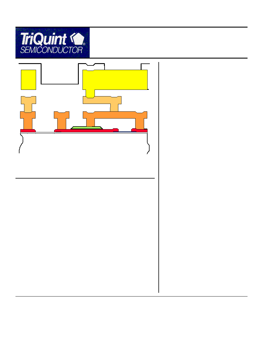
TQTRx Process Cross-Section
Production Process
TQRLC
Advanced Passives Foundry Service
Features
·
Thick 4 Layer Metal; > 9 µm total
thickness
·
High Density Interconnects:
·
3 Global
·
1 Local
·
High-Q Passives; Inductor Q >50
@ 2 GHz
·
Low Cost: Passives Only
·
Thin Film Resistors
·
Dielectric Encapsulated Metals
·
Planarized Surface;
simplified plastic packaging
·
Substrate Vias Available
·
Volume Production Process
Applications
·
Passive Components:
·
Phase Shifters
·
Baluns
·
Transformers
·
Couplers
·
Mixers
(with off-chip di-
ode arrays)
·
Circuits Requiring High-Q
Passive Elements
·
Matching Circuits
·
RF Module Front-End Filters
·
General RF and Microwave Imped-
ance Matching
General Description
TriQuint's TQRLC is a pure passives process. It is targeted at
high performance, small size passive-only circuits and utilizes
over 9 µm of gold metal. High density interconnections are ac-
complished with three thick global and one surface metal inter-
connect layers. The four metal layers are encapsulated in a high
performance, low dielectric constant material that allows wiring
flexibility and plastic packaging simplicity. Precision NiCr resis-
tors, inductors, and high value MIM capacitors are available.
The process is based on the TQTRx process, currently
TriQuint's highest volume process. The TQRLC process is
available on 150-mm (6 inch) wafers.
Semiconductors for Communications
www.triquint.com
TriQuint Semiconductor
2300 NE Brookwood Pkwy
Hillsboro, Oregon 97124
Phone: 503-615-9000
Fax: 503-615-8905
Email: info@triquint.com
Page 1 of 3; Rev 2.1 8/10/02
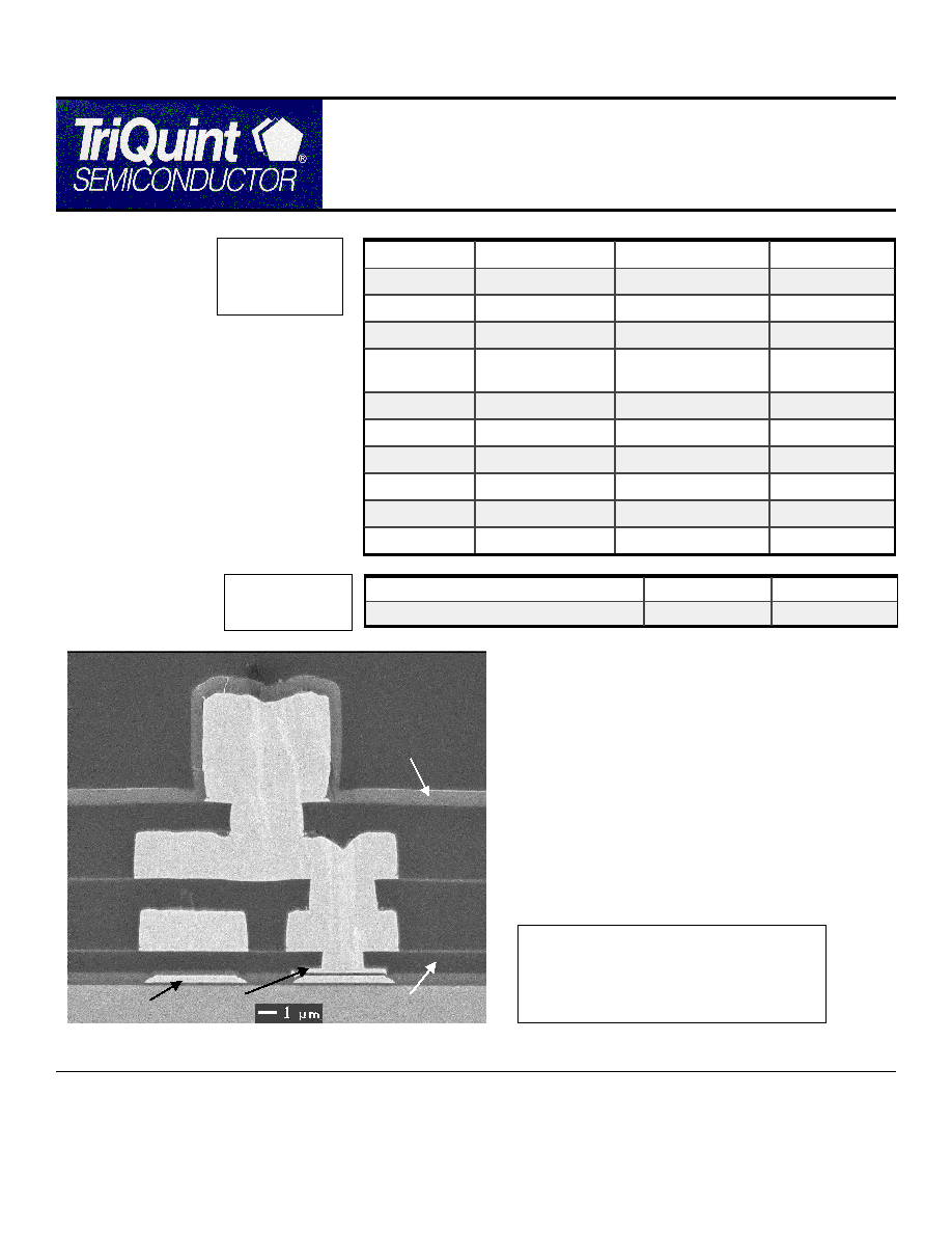
TQRLC Process Cross-Section
NiCr Resistor
MIM Capacitor
Low-cost Mechanical Grade Semi-Insulating GaAs Substrate
MIM Metal
Metal 0
Metal 1
Metal 1
Metal 1 - 2 um
Passivation Via
Metal 2
Metal 3
Dielectric
Dielectric
Metal 3 - 5 um
Metal 2 - 2 um
NiCr Resistor
MIM Capacitor
Low-cost Mechanical Grade Semi-Insulating GaAs Substrate
MIM Metal
Metal 0
Metal 1
Metal 1
Metal 1 - 2 um
Passivation Via
Metal 2
Metal 3
Dielectric
Dielectric
Metal 3 - 5 um
Metal 2 - 2 um
Released Process
TQTRx
MESFET Foundry Service
Semiconductors for Communications
www.triquint.com
TriQuint Semiconductor
2300 NE Brookwood Pkwy
Hillsboro, Oregon 97124
Phone: 503-615-9000
Fax: 503-615-8905
Email: info@triquint.com
Page 2 of 7; Rev 1.0 11/15/01
Specifications Subject to Change
Capacitor Breakdown Voltage - Design
20
V
- Typical
40
V
Maximum
Ratings
Production Process
TQRLC
Advanced Passives Foundry Service
Semiconductors for Communications
www.triquint.com
TriQuint Semiconductor
2300 NE Brookwood Pkwy
Hillsboro, Oregon 97124
Phone: 503-615-9000
Fax: 503-615-8905
Email: info@triquint.com
Page 2 of 3; Rev 2.1 8/10/02
Element
Parameter
Value
Units
Interconnects Metal Layers
Four: 0.4,2,2,5.3
µm
Space Width
Met3= 3; Met1&2= 2
µm
Trace Width
Met3= 5; Met1&2= 2
µm
BCB Dielectric Nom. Thickness
ILD1= 1 +/-0.1;
ILD2&3= 3.2 +/- 0.2
µm
Dielectric Constant
2.8
MIM Caps
Values
600
pF/mm2
Resistors
NiCr
50
Ohms/sq
Vias
Yes
Mask Layers
No Vias
12
With Vias
14
TQRLC
Process
Details
Met3
Via3
Met2
Via2
Via1
Met1
Met0
MIM
ILD3
dielectric
ILD2
dielectric
ILD1 dielectric
Passivation
Example of Metal Stack Configurations
Possible with TQRLC Process; Edge or
Parallel-Coupled Structures Through
The ILD Layers Are Also Possible.
Design Tool Status
·
Design Manual Available Now
·
Device Library of Circuit Elements includes Thin Film
Resistors, Capacitors, Inductors
·
Agilent ADS Definition File for E-M Simulation Now
·
Layout/Verification Kit for ICEditors
·
Cadence Layout Library Available Q3'02
Process Qualification
Status
·
TQRLC is a fully-released process
·
Reliability Reports
·
TQRLC Process Qualification
·
TQTRx Element Qualification Report
·
For more information on Quality and
Reliability, contact TriQuint or visit:
www.tqs.com/Manufacturing/QR/bdy_qr-pubs.htm.
Production Process
TQRLC
Advanced Passives Foundry Service
Semiconductors for Communications
www.triquint.com
TriQuint Semiconductor
2300 NE Brookwood Pkwy
Hillsboro, Oregon 97124
Phone: 503-615-9000
Fax: 503-615-8905
Email: info@triquint.com
Page 3 of 3; Rev 2.1 8/10/02
Applications Support Services
·
Tiling of GDSII Stream Files including PCM
·
Design Rule Check Services
·
Layout versus Schematic Check Services
·
Engineering Services:
·
Packaging Development
·
Test Development Engineering (on-wafer and
packaged parts)
·
Thermal Analysis Engineering
·
Yield Enhancement Engineering
·
Part Qualification Services
·
Failure Analysis
Manufacturing Services
·
Mask Making
·
Production 150 mm Wafer Fab
·
Wafer Thinning
·
Wafer Sawing
·
Substrate Vias
·
DC Die Sort Testing
·
RF On-Wafer Testing
·
Plastic Packaging
·
RF Packaged Part Testing
Please contact your local TriQuint Semiconductor Representative or
Foundry Services Staff for additional information:
E-mail: sales@triquint.com Phone: (503) 615-9000 Fax: (503) 615-8905
Prototyping and Development
·
Prototype Development Quickturn (PDQ):
·
Shared Mask Set;
·
Run Monthly;
·
Hot Lot Cycle Time;
·
Via and Non-Via Options.
·
Prototype Wafer Option (PWO):
·
Customer-specific Masks, Customer Schedule
·
2 wafers delivered
·
Hot Lot Cycle Time
·
With thinning and sawing; optional backside
vias
Training
·
GaAs Design Classes:
·
Half Day Introduction; Upon Request
·
Four Day Technical Training; Fall & Spring at
TriQuint Oregon facility
·
For Training Schedules, please visit:
www.triquint.com/foundry/