 | –≠–ª–µ–∫—Ç—Ä–æ–Ω–Ω—ã–π –∫–æ–º–ø–æ–Ω–µ–Ω—Ç: 1233 | –°–∫–∞—á–∞—Ç—å:  PDF PDF  ZIP ZIP |

UNISONIC TECHNOLOGIES CO., LTD
1233
LINEAR INTEGRATED CIRCUIT
www.unisonic.com.tw
1
Copyright © 2005 Unisonic Technologies Co., LTD
QW-R107-023,E
DUAL 3-W BTL AUDIO POWER
AMPLIFIER
DESCRIPTION
The UTC
1233
is an audio power amplifier IC for the stereo
system. In the BTL (balanced transformerless) method, fewer
external parts and easier design for applications are required.
FEATURES
* 3-W output (8) with supply voltage of 8V
* On-chip standby function
* On-chip volume function
H S IP -12A
H S IP -14B
*Pb-free plating product number: 1233L
ORDERING INFORMATION
Ordering Number
Normal Lead
Free
Plating
Package Packing
1233-F12-T 1233L-F12-T
HSIP-12A
Tube
1233-H14-B-T 1233L-H14-B-T
HSIP-14B Tube
1233
LINEAR INTEGRATED CIRCUIT
UNISONIC TECHNOLOGIES CO., LTD
2
www.unisonic.com.tw
QW-R107-023,,E
PIN DESCRIPTION
PIN NO.
HSIP-12A HSIP-14B
PIN NAME
DESCRIPTION
1 NC
No
connect
1 2
V
CC
Supply
voltage
2
3
Ch.1+ output
Ch.1+ output
3
4
GND
Ground (output ch.1)
4 5
Ch.1-
output
Ch.1
- output
5
6
Standby
Standby (standby state if this pin is open)
6
7
Ch.1 input
Ch.1 input
7 8 GND
Ground
(input)
8
9
Ch.2 input
Ch.2 input
9
10
Volume
Volume (max. volume if this pin is open.)
10
11
Ch.2- output
Ch.2 - output
11
12
GND
Ground (output ch.2)
12 13
Ch.2+
output
Ch.2
+ output
14 NC
No
connect
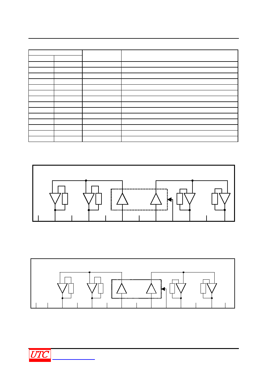
BLOCK DIAGRAM
HSIP-12A
+
-
+
-
Vc
c
C
h
.1+
out
pu
t
GN
D
(
C
h
.
1
ou
tput
)
C
h
.
1
-
o
u
t
put
S
t
and
by
C
h
.
1
i
nput
GN
D
C
h
.2
i
n
p
u
t
Vo
lu
m
e
Ch
.2
-
o
u
t
p
u
t
GND
(
C
h.
2 o
u
tp
ut
)
Ch
.
2
+
o
u
tp
u
t
1
2
3
4
5
6
7
8
9
10
11
12
-
-
+
+
HSIP-14B
+
-
+
-
Vc
c
C
h
.
1+
o
u
t
p
u
t
GN
D
(
C
h.
1
ou
t
p
u
t
)
C
h
.
1
-
out
p
u
t
S
t
andby
C
h
.1
i
np
ut
GN
D
C
h
.2
i
n
put
Vo
l
um
e
C
h
.
2
-
o
ut
put
GN
D
(
C
h.
2
out
p
u
t
)
C
h
.
2+
o
u
t
p
u
t
2
3
4
5
6
7
8
9
10
11
12
13
-
-
+
+
14
1

1233
LINEAR INTEGRATED CIRCUIT
UNISONIC TECHNOLOGIES CO., LTD
3
www.unisonic.com.tw
QW-R107-023,,E
ABSOLUTE MAXIMUM RATINGS
(Ta = 25)
PARAMETER SYMBOL
RATINGS
UNIT
Supply Voltage (At no signal)
V
CC
14 V
Supply Current
I
CC
2.0 A
Power Dissipation(Ta = 70)
P
D
1.92 W
Operating Temperature
T
OPR
0 ~ +70
∞C
Storage Temperature
T
STG
-40 ~ +150
∞C
Note:1.Absolute maximum ratings are those values beyond which the device could be permanently damaged.
Absolute maximum ratings are stress ratings only and functional device operation is not implied.
2.The device is guaranteed to meet performance specification within 0~70 operating temperature range
and assured by design from ≠40~85.
RECOMMENDED OPERATING RATINGS
PARAMETER SYMBOL
RATINGS
UNIT
Supply voltage
Vcc
3.5 ~ 13.5
V
ELECTRICAL CHARACTERISTICS
(Vcc=8.0V, R
L
=8, f=1kHz, Ta=25±2, unless otherwise specified.)
PARAMETER SYMBOL
TEST
CONDITIONS
MIN
TYP
MAX
UNIT
Quiescent Circuit Current
I
D
V
IN
=0mV, Vo1.=0V
45
100
mA
Standby Current
I
STN-BY
V
IN
=0mV, Vo1.=0V
1
10
A
Output Noise Voltage*
V
NO
R
G
=10k, Vo1.=0V
0.10
0.4
mV(rms)
Output Offset Voltage
V
OFF
R
G
=10k, Vo1.=0V
-250
0
250
mV
Total Harmonic Distortion
THD
P
OUT
=0.5W, Vo1.=1.25V
0.10
0.5
%
Maximum Output Power
P
OUT1
THD=10%,
Vo1.=1.25V
2.4 3.0
W
Ripple Rejection*
RR
R
G
=10k, Vo1.=0V
V
R
=1V(rms), f
R
=120Hz
30 50 dB
Voltage Gain
G
v
P
OUT
=0.5W, Vo1.=1.25V
31
33
35
dB
Volume Attenuation Rate*
Att
P
OUT
=0.5W, Vo1.=0V
70
85
dB
Channel Balance 1
CB1
P
OUT
=0.5W, Vo1.=1.25V
-1
0
1
dB
Channel Balance 2
CB2
P
OUT
=0.5W, Vo1.=0.6V
-3
0
3
dB
Intermediate Voltage Gain
G
VM
P
OUT
=0.5W, Vo1.=0.6V
20.5
23.5
26.5
dB
Channel Crosstalk
C
T
P
OUT
=0.5W, Vo1.=1.25V
40
55
dB
* In measuring, the filter for the range of 15 Hz ~ 30 kHz (12 dB/OCT) is used.
1233
LINEAR INTEGRATED CIRCUIT
UNISONIC TECHNOLOGIES CO., LTD
4
www.unisonic.com.tw
QW-R107-023,,E
TERMINAL EQUIVALENT CIRCUITS AT V
CC
=8V
PIN NO.
HSIP-12A HSIP-14B
PIN NAME
VOLTAGE
1 2
Vcc
8V
2
3
Ch.1 + output pin
3.6V (at no signal)
3 4
GND
0V
4
5
Ch.1 - output pin
3.6V (at no signal)
5 6 Standby
pin
0V or 5V (Standby off at supply 5V.
Standby at 0.4V less or open. )
6
7
Ch.1 input pin
1.4V (Input circuit bias voltage is output)
7 8
GND
0V
8
9
Ch.2 input pin
1.4V (Input circuit bias voltage is output)
9
10
Volume pin
Supply to 0V ~ 1.25V
10
11
Ch.2-output pin
3.6V (at no signal)
11 12
GND
0V
12
13
Ch.2+ output pin
3.6V (at no signal)
USAGE NOTES
* Please avoid the short-circuits to V
CC
, ground, or load short-circuit.
* Please connect the cooling fin with the GND potential.
* The thermal shutdown circuit operates at about T
J
=150 . However, the thermal shutdown circuit is reset
automatically if the temperature drops.
* Please carefully design the heat radiation especially when you take out high power at high V
CC
.
* Please connect only the ground of signal with the signal GND of the amplifier in the previous stage.
1233
LINEAR INTEGRATED CIRCUIT
UNISONIC TECHNOLOGIES CO., LTD
5
www.unisonic.com.tw
QW-R107-023,,E
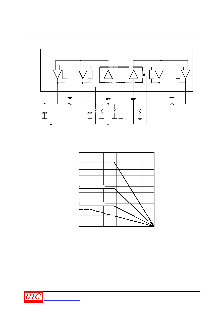
APPLICATION CIRCUIT EXAMPLE
+
-
+
-
1
2
3
4
5
6
7
8
9
10
11
12
-
-
+
+
470 F
Vcc
8
Out 1
10F
+
+
68
k
270
k
10
k
Standby
V
IN1
1.0F
+
1.0F
+
10
k
V
IN2
Volume
8
Out 2
TECHNICAL DATA (
HSIP-12A)
13
25
0
70
50
7
9
12
11
8
6
P
D
- Ta
P
o
w
e
r
D
i
s
s
ip
a
t
io
n
,
P
D
(m
W
)
10
75
100
5/W heat sink
5
4
125
150
10/W heat sink
20/W heat sink
Independent IC
without heat sink
JA
=41.7/W
3
2
1
0