UTC 2SB772S
PNP EPITAXIAL SILICON TRANSISTOR
UTC
UNISONIC TECHNOLOGIES CO. LTD
1
MEDIUM POWER LOW VOLTAGE
TRANSISTOR
DESCRIPTION
The UTC 2SB772S is a medium power low voltage
transistor, designed for audio power amplifier, DC-DC
converter and voltage regulator.
FEATURES
*High current output up to 3A
*Low saturation voltage
*Complement to 2SD882S
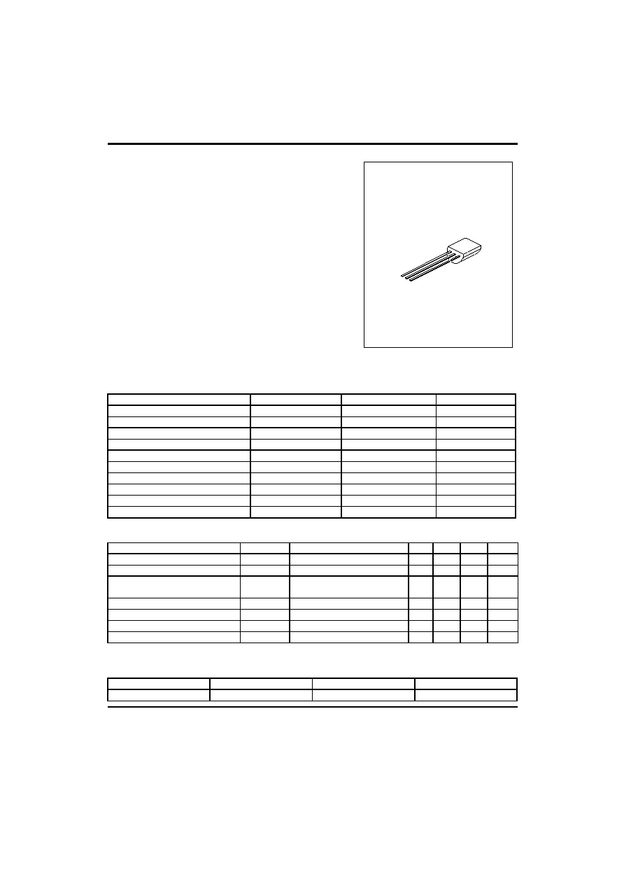
TO-92
1
1:EMITTER 2:COLLECTOR 3:BASE
ABSOLUTE MAXIMUM RATINGS
( Ta=25
∞
C ,unless otherwise specified )
PARAMETER
SYMBOL
VALUE
UNIT
Collector-Base Voltage
V
CBO
-40
V
Collector-Emitter Voltage
V
CEO
-30
V
Emitter-Base Voltage
V
EBO
-5
V
Collector Dissipation( Tc=25
∞
C)
Pc
10
W
Collector Dissipation( Ta=25
∞
C)
Pc
1
W
Collector Current(DC)
Ic
-3
A
Collector Current(PULSE)
Ic
-7
A
Base Current
I
B
-0.6
A
Junction Temperature
T
j
150
∞
C
Storage Temperature
T
STG
-55 ~ +150
∞
C
ELECTRICAL CHARACTERISTICS
(Ta=25
∞
C,unless otherwise specified)
PARAMETER
SYMBOL
TEST CONDITIONS
MIN
TYP
MAX
UNIT
Collector Cut-Off Current
I
CBO
V
CB
=-30V,I
E
=0
-1000
nA
Emitter Cut-Off Current
I
EBO
V
EB
=-3V,Ic=0
-1000
nA
DC Current Gain(note 1)
h
FE1
h
FE2
V
CE
=-2V,Ic=-20mA
V
CE
=-2V,Ic=-1A
30
100
200
150
400
Collector-Emitter Saturation Voltage
V
CE
(sat)
Ic=-2A,I
B
=-0.2A
-0.3
-0.5
V
Base-Emitter Saturation Voltage
V
BE
(sat)
Ic=-2A,I
B
=-0.2A
-1.0
-2.0
V
Current Gain Bandwidth Product
f
T
V
CE
=-5V,Ic=-0.1A
80
MHz
Output Capacitance
Cob
V
CB
=-10V,I
E
=0,f=1MHz
45
pF
Note 1:Pulse test:PW<300
µ
s,Duty Cycle<2%
CLASSIFICATION OF hFE
RANK
Q
P
E
RANGE
100-200
160-320
200-400
UTC 2SB772S
PNP EPITAXIAL SILICON TRANSISTOR
UTC
UNISONIC TECHNOLOGIES CO. LTD
2
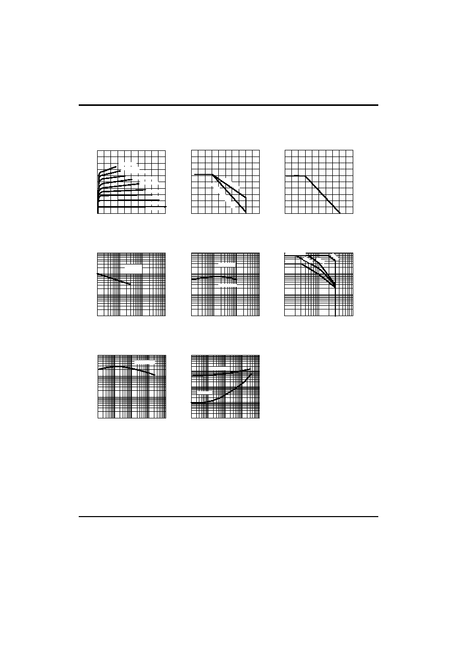
TYPICAL PERFORMANCE CHARACTERISTICS
Fig.1 Static characteristics
-Collector-Emitter voltage(V)
-Ic,Collector current(A)
0
4
8
12
16
20
0
0.4
0.8
1.2
1.6
Tc,Case Temperature(
¢X
C)
-IB=1mA
-IB=2mA
-IB=3mA
-IB=4mA
-IB=5mA
-IB=6mA
-IB=7mA
-IB=8MA
-IB=9mA
Fig.2 Derating curve of safe
operating areas
- Ic Derating(%)
200
150
100
50
0
-50
0
50
100
150
S/b limited
Dissipation limited
Tc,Case Temperature(
¢X
C)
200
150
100
50
0
-50
Fig.3 Power Derating
Power Dissipation(W)
0
4
8
12
Fig.4 Collector Output
capacitance
-Collector-Base Voltage(v)
Output Capacitance(pF)
10
0
10
-1
10
-2
10
-3
10
1
10
2
10
3
10
0
I
E
=0
f=1MHz
Fig.5 Current gain-
bandwidth product
F
T
(MHz), Current gain-
bandwidth product
10
1
10
2
10
3
10
0
V
CE
=5V
Collector-Emitter Voltage
-Ic,Collector current(A)
Fig.6 Safe operating area
Ic(max),DC
Ic(max),Pulse
10mS
1mS
0.1mS
Ic,Collector current(A)
Fig.7 DC current gain
-Ic,Collector current(mA)
-Ic,Collector current(mA)
Fig.8 Saturation Voltage
DC current Gain,H
FE
10
1
10
2
10
3
10
0
-Saturation Voltage(mV)
V
CE
=-2V
V
CE
(sat)
V
BE
(sat)
10
-2
10
-1
10
0
10
1
10
-2
10
-1
10
0
10
1
10
0
10
1
10
2
10
0
10
1
10
2
10
3
10
4
10
0
10
1
10
2
10
3
10
4
10
0
10
1
10
2
10
3
10
4
I
B
=8mA
I
B
=8mA