 | –≠–ª–µ–∫—Ç—Ä–æ–Ω–Ω—ã–π –∫–æ–º–ø–æ–Ω–µ–Ω—Ç: KA7524 | –°–∫–∞—á–∞—Ç—å:  PDF PDF  ZIP ZIP |

UTC KA7524
LINEAR INTEGRATED CIRCUIT
UTC
UNISONIC TECHNOLOGIES CO., LTD.
1
QW-R114-001,A
POWER FACTOR CONTROLLER
DESCRIPTION
The UTC KA7524 provides the necessary features to
implement the Electronic BALLAST control and S.M.P.S
application for designing active power factor correction circuit
FEATURES
*Internal self-starting
*Micro power start up mode
*Included under voltage lockout circuit
*Internal 1% reference
*High output current: peak 500mA
DIP-8
BLOCK DIAGRAM

UTC KA7524
LINEAR INTEGRATED CIRCUIT
UTC
UNISONIC TECHNOLOGIES CO., LTD.
2
QW-R114-001,A
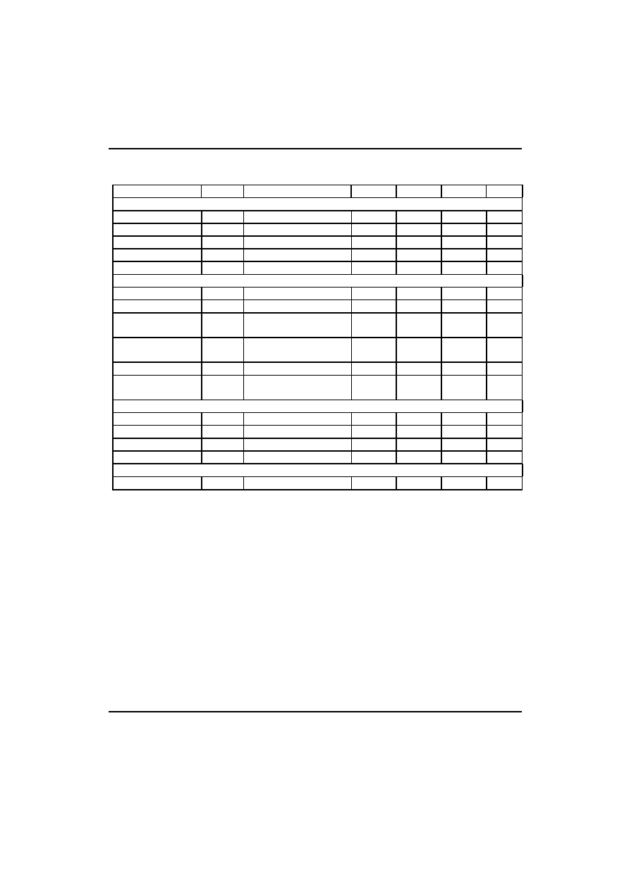
ABSOLUTE MAXIMUM RATINGS
(Ta=25
∞
C)
PARAMETER
SYMBOL
VALUE
UNIT
Supply Voltage
Vcc
20
V
Peak Driver Output Current
Io(p)
500
mA
Detect Clamping Diode Current
Idet
10
mA
Output Clamping Diode Current
Io(c.d)
10
mA
Operating Temperature
Topr
-45~65
∞
C
Storage Temperature
Tstg
-65~150
∞
C
ELECTRICAL CHARACTERISTICS
(Ta=25
∞
C)
(All voltage referenced to GND unless othrewise specified)
PARAMETER
SYMBOL
TEST CONDITIONS
MIN
TYP
MAX
UNIT
Under Voltage Lockout Section
Start Threshold Voltage
Vth(st)
9.2
10
10.8
V
UV lockout Hysteresis
Vths
1.8
2.0
2.2
V
Supply Zener Voltage
Vz
17
V
Supply Current Section
Start-up Supply Current
Istart
Vcc<Vth
0.25
0.5
mA
Operating Supply
Current
Icc
Vcc=12V,No load
6
12
mA
Dynamic Operating
Current
Icc(d)
Vcc=12V,f=50KHZ,
Cgs=1000pF
10
20
mA
Reference Section (note 1)
Reference Voltage
Vref
2.475
2.5
2.525
V
Line Regulation
Vref
12V<Vcc<16V
0.1
10
mV
Load Regulation
Vref
0<Iref<2mA
0.1
10
mV
Temperature Stability
STt
20
mV
Error Amplifier Section
Input Offset Voltage
Vio
-15
15
mV
Input Bias Current
Ibias
-1
-0.1
1
µ
A
Large Signal Open Loop
gain
Gv
60
100
dB
Power Supply Rejection
Ratio
PSRR
60
86
dB
Output Current
Isource
2
mA
Isink
-2
mA
Output Voltage range
Vo(p)
1.2
4
V
Unity Gain Bandwidth
UBW
1.0
MHZ
Phase Margin
MPH
57
∞
C
UTC KA7524
LINEAR INTEGRATED CIRCUIT
UTC
UNISONIC TECHNOLOGIES CO., LTD.
3
QW-R114-001,A
ELECTRICAL CHARACTERISTICS
(Ta=25
∞
C) (continued)
PARAMETER
SYMBOL
TEST CONDITIONS
MIN
TYP
MAX
UNIT
Multiplier Section
M1 Input Voltage Range
Vi(m1)
0
2
V
M2 Input Voltage Range
Vi(m2)
Vref
Vref+1
V
Input Bias Current
I
bias
-2
-0.5
2
µ
A
Multiplier Gain
Gv
Vi(m1)=0.5V,Vi(m2)=3V
0.8
/V
Multiplier Gain Stability
STt
-0.2
%/
∞
C
Current Sense Section
Input Voltage Threshold
Vth
1.0
1.3
1.6
V
Hysteresis
Vths
200
mV
Input Low Clamp
Voltage
Vic(L)
Idet=0mA
0.95
V
Input High Clamp
Voltage
Vic(H)
Idet=3mA
6.1
7.1
V
Input Current
Ii
0.8V<Vdet<6V
5
µ
A
Input Clamp Diode
Current
Icd
Vdet<0.9V,Vdet>6V
3
mA
Current Detect Section
Output Voltage(High)
Vo(H)
Io=-10mA,Vcc=12V
7
9
V
Output Voltage(low)
Vo(L)
Io=10mA,Vcc=12V
0.8
1.8
V
Rising Time
tr
C
L
=1000pF
100
200
ns
Failing Time
tf
C
L
=1000pF
90
200
ns
Self-Start Section
Self Starting Time
tss
12
µ
s
NOTE:
1.Reference can not be tested on the PKG
2.Gv=Vo(m)/(Vi(m1)*(Vi(m2)-Vref))
UTC KA7524
LINEAR INTEGRATED CIRCUIT
UTC
UNISONIC TECHNOLOGIES CO., LTD.
4
QW-R114-001,A
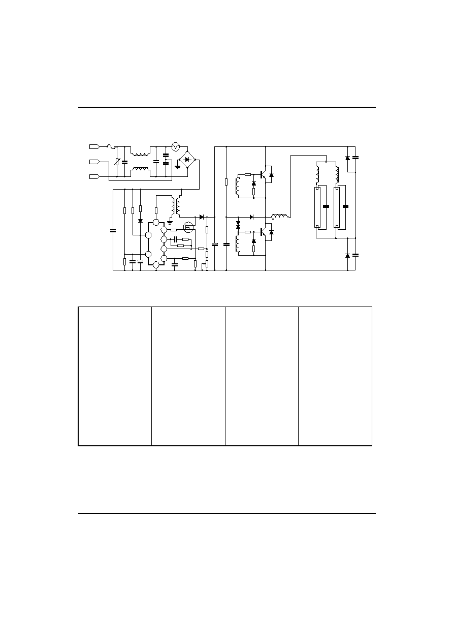
APPLICATION CIRCUIT
H
N
F.G
5
7
2
1
4
8
3
6
2A
TNR
C1
L1
R3
C2
C4
C3
NTC
R1
R4
D1
R5
C5
T1
Q1
D2
R6
R7
R8
R9
R10
R11
R12
VR1
C6 C7
R2
C10
C11
T2
DIAC
D9
Q2
D6
D4
R19
D8
C15
C13
C12
D7
C14
L2
L3
D5
Q3
D3
R17
R16
T2
R14
BDI
R18
T2
LAMP TUBE 1
C9
C8
R13
LAMP TUBE 1
PART LIST
Resistor
R16 5.1
C10 47
µ
F/450V
D6 FR107
R1 1.8M
R17 27
C11 0.1
µ
F
D7 FR107
R2 10K
R18 5.1
C12 3300pF
D8 FR107
R3 100K
R19 27
C13 3300pF
BD1 PBP204
R4 3.3
¶ ∏
VR1 5K
C14 0.01
µ
F
TNR 12G471
R5 22K
NTC 10
C15 0.01
µ
F
DIAIC 32V
Capacitor
Semiconductor
Magnetics
R7 2.2K
C1 0.1
µ
F
IC1 UTC KA7524
T1 E1-25(PC30):P=70T
R8 2.2M
C2 0.1
µ
F
Q1 IRF830
S=4T,Gap=0.5mm
R9 150K
C3 4700pF
Q2 2SC5039
T2 D15(GP-5):
R10 330
¶ ∏
C4 4700pF
Q3 2SC5039
P=3T,S=13T
R11 0.75
¶ ∏
C5 0.1
µ
F
D1 1N4004
L1 EE-25(Iron Power)
R12 5.1K
C6 0.01
µ
F
D2 1N4937
80mH
R13 1M
C7 100
µ
F
D3 1N4148
L2 EI-25(PC30):
R14 390K
C8 0.1
µ
F
D4 1N4148
150T,Gap=0.4mm
R15 3.9M
C9 3300pF
D5 FR107