 | –≠–ª–µ–∫—Ç—Ä–æ–Ω–Ω—ã–π –∫–æ–º–ø–æ–Ω–µ–Ω—Ç: MC33092 | –°–∫–∞—á–∞—Ç—å:  PDF PDF  ZIP ZIP |
UTC MC33092 LINEAR INTEGRATED CIRCUIT
UTC
UNISONIC TECHNOLOGIES CO., LTD.
1
QW-R121-006,A
ALTERNATOR VOLTAGE
REGULATOR
DESCRIPTION
The MC33092 is specifically designed for voltage
regulation and Load Response Control (LRC) of diode
rectified alternator charging systems, as commonly
found in automotive applications.
In maintaining system voltage, the MC33092
monitors and compares the system battery voltage to
an externally programmed set point value and pulse
width modulates an N≠channel MOSFET transistor to
control the average alternator field current.
FEATURE
*Forced Load Response Control (LRC) with Heavy
Load Transitions at Low RPM
*Capable of Regulating Voltage to
± 0.1 V @ 25∞C
*Operating Frequency Selectable with One External
Resistor
*< 0.1 V Variation over Speed Range of 2000 to
10,000 RPM
*< 0.4 V Variation over 10% to 95% of Maximum
Alternator Output
*Maintains Regulation with External Loads as Low as
1.0 A
*Load Dump Protection of Lamp, Field Control
Devices, and Loads
*Duty Cycle Limit Protection
*Provides High Side MOSFET Control of a Ground
Referenced Field Winding
*Controlled MOSFET and Flyback Diode Recovery
Characteristics for Minimum RFI
*Optional 2.5 or 10 sec. LRC Rate Control (Osc. Freq.
= 280 kHz)
*Undervoltage, Overvoltage and Phase Fault (Broken
Belt) Detection
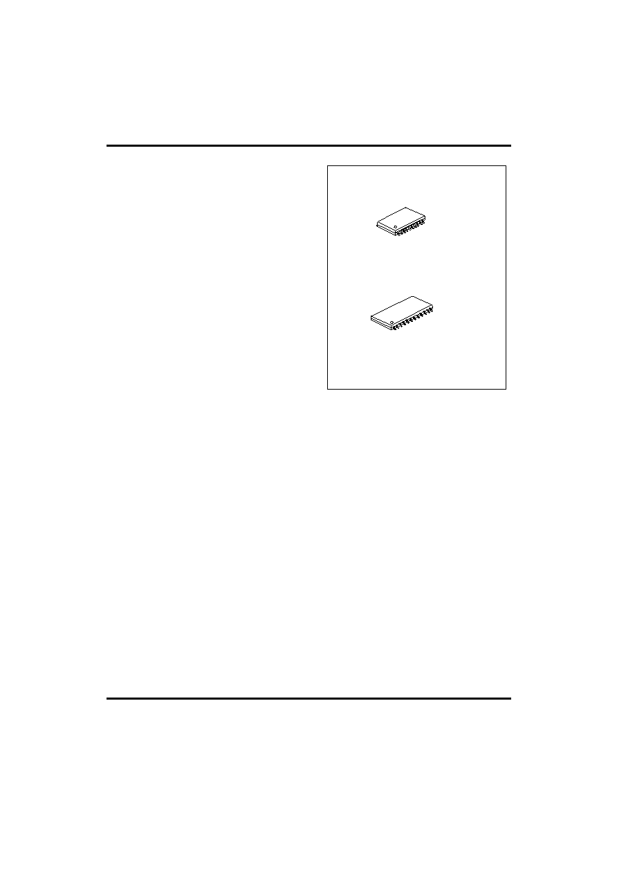
SOP-24
SOP-20
UTC MC33092 LINEAR INTEGRATED CIRCUIT
UTC
UNISONIC TECHNOLOGIES CO., LTD.
2
QW-R121-006,A
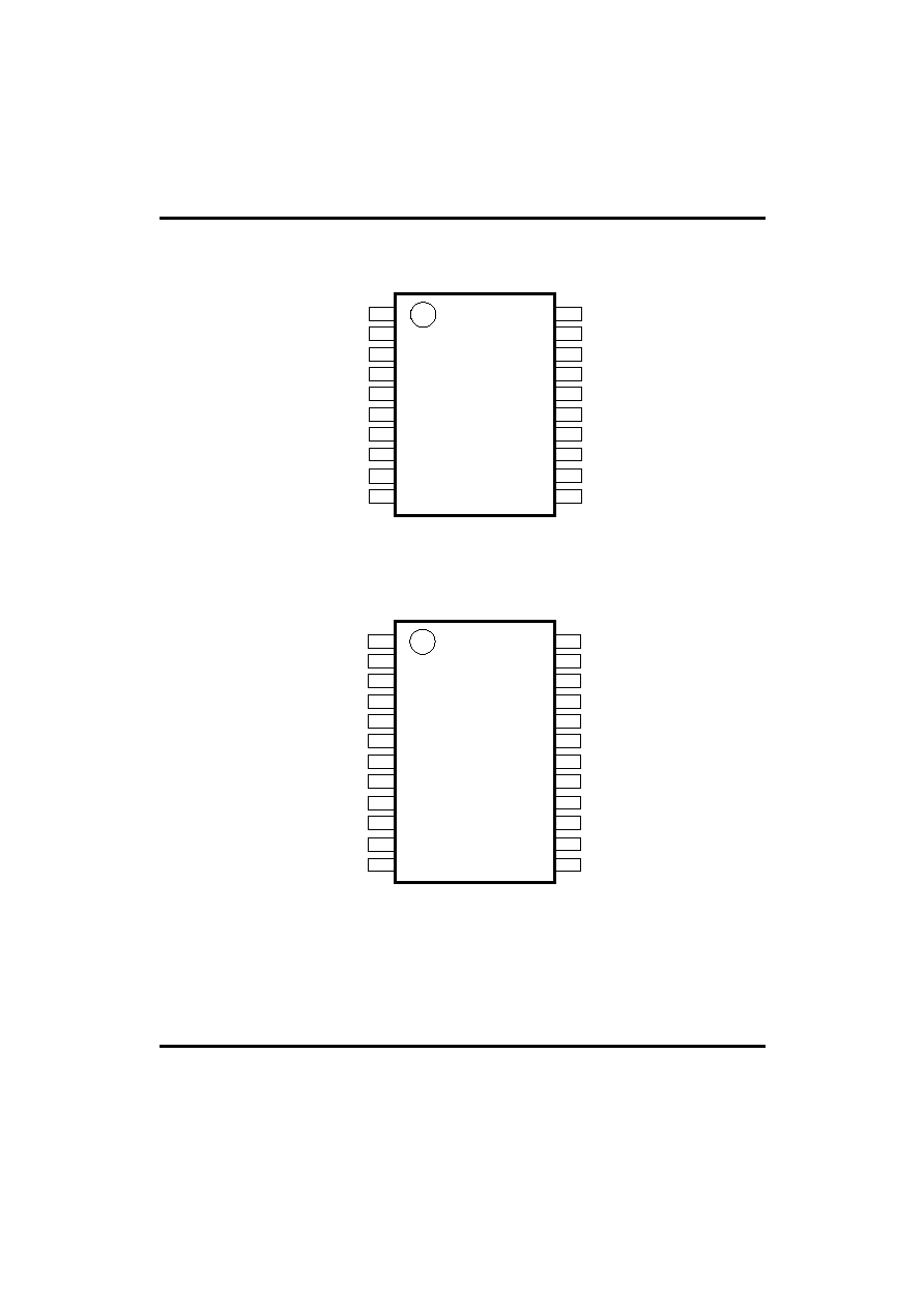
PIN CONFIGURATION
20-pin Package
12
11
9
10
2
1
20
19
18
17
16
15
14
13
5
6
7
8
4
3
O s c illator A djus t
R emote S ens e
Filter B uf f er
Lamp B as e
Lamp C ollec tor
P has e
V r ef 0
O s c illator
G N D
G N D
G ate
S our c e
U nder voltage
V r ef
G N D
R at e
Supply R egulation
V c c 3
V c c 1
N C
24-pin Package
14
13
11
12
16
15
9
10
2
1
24
23
22
21
20
19
18
17
5
6
7
8
4
3
O s c illator A djus t
R emote S ens e
Filter B uf f er
Lamp B as e
Lamp C ollec t or
P has e
V r ef 0
O s c illator
G N D
N C
G N D
N C
N C
N C
G ate
S our c e
U nder volt age
V r ef
G N D
R ate
Supply R egulation
Vc c 3
V c c 1
N C
UTC MC33092 LINEAR INTEGRATED CIRCUIT
UTC
UNISONIC TECHNOLOGIES CO., LTD.
3
QW-R121-006,A
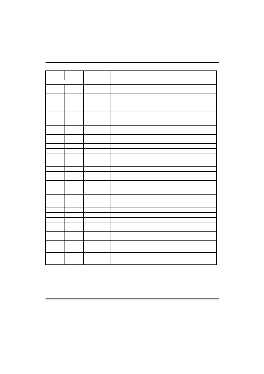
PIN DESCRIPTION
20-pin
Package
24-pin
Package
PIN No.
PIN NAME
DESCRIPTION
1 1 FB
This pin provides a filtered result of the Sense input (if the Sense input
is used) or the Supply Regulation input (if the Sense input is not used).
2 2 Sense
The Sense input is a remote, low current battery voltage reference
input used to give an accurate representation of the true battery
voltage. This input is also used to monitor overvoltage or load dump
conditions.
3
3
Lamp Collector
and
Power-Up/Down
This pin connects to the collector of the transistor (Q2) used to drive
the fault lamp. It is also used to sense a closed ignition switch (voltage
sense) which then turns power on to the IC.
4 4
Lamp
Base
The Lamp Base pin provides base current to the fault lamp drive
transistor (Q2).
5 5 Ground
Grounded to provide a ground return for the fault lamp control logic
circuit.
6, 15
6,15
Ground
IC ground reference pins.
7
7
Oscillator Adjust A resistor to ground on this pin adjusts the internal oscillator frequency.
8 8 Vref0
*
This is a test point for the 1.1 V to 1.4 V reference voltage. It has a zero
temperature coefficient. The reference is used internally for phase
signal and undervoltage detection.
9
9
Oscillator *
Test point for checking the operation of the internal oscillator.
10 10 Phase
The Phase input detects the existence of a magnetic field rotating
within the alternator.
11 11 Rate
The Rate pin is used to select a slow mode (floating) or fast mode
(ground) Load
Response Control recovery rate.
12 12
Supply
Regulation
The voltage on the Supply Regulation pin is used as a representation
of the alternator output voltage. This input also used to monitor
overvoltage or load dump conditions.
13
13
VCC3
Positive supply for the internal Charge Pump.
14
14
VCC1
Positive supply for the entire IC except for the Charge Pump.
15,6
15,6
Ground
Ground reference for the IC.
16
16,17,18,
19,20
N/C
No connection.
17
21
Gate
Controls the Gate of the MOSFET used to energize the field winding.
18
22
Source
Field winding control MOSFET source reference.
19
23 Undervoltage
If the voltage at this pin goes below 1.0 V, the fault lamp is guaranteed
to turn on. The IC will continue to function, but with limited
performance.
20
24** Vref
*
Test point for the 1.7 V to 2.3 V Bandgap reference voltage. This
voltage has a negative temperature coefficient of approximately ≠11
mV/
∞C.
NOTE: *
Pins 8, 9 and 20(24**) are test points only.
** For 24-pin package.
UTC MC33092 LINEAR INTEGRATED CIRCUIT
UTC
UNISONIC TECHNOLOGIES CO., LTD.
4
QW-R121-006,A
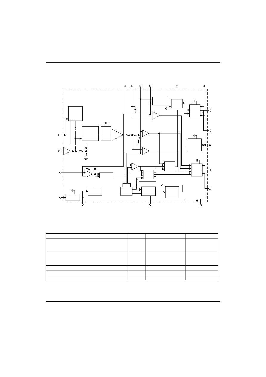
BLOCK DIAGRAM
Lost
Sense
Circuit
Signal
Combiner
and Switch
Low
Pass
Filter
Counter
Bandgap
Reference
Power
Supply
Output
Control
Lamp
Control
Logic
Charge
Pump
Power
Up/Down
Circuit
Oscillator
Control
Logic
Divide By
(1/12/48)
Counter
(2
8
)
DAC
Up/Down
Counter
(2
4
)
Prescaler
(2
4
)
MC33092
1
FB
19
UV
20
Vref
8
Vref0
Vcc1
14
Vcc3
13
17
Gate
18
Source
3
Lamp
Coll.
4
Lamp
Base
5
Gnd
6
Gnd
15
11
Rate
9
Oscillator
7
Osc.
Adjust
10
Phase
12
Supply
Reg
(Local)
2
Sense
(Remote)
Buff
X1
+
-
+
-
+
-
+
-
+
-
Bias
Undervoltage
Load Dump
Overvoltage
Regulate
12
4
8
23** 24**
21**
22**
+
Note: ** For 24-pin package
ABSOLUTE MAXIMUM RATINGS
PARAMETER SYMBOL
RATINGS
UNIT
Power Supply Voltage
Load Dump Transient Voltage (Note 1)
Negative Voltage (Note 2)
Vbat
+Vmax
≠Vmin
24
40
-2.5
V
Power Dissipation (Ta = 125
∞C)
SOP-20
SOP-24
P
D
867
1000
mW
Operating Ambient Temperature
Ta
-40 ~ +125
∞C
Operating Junction Temperature
Tj
+150
∞C
Storage Temperature
Tstg
-45 ~ +150
∞C
NOTES:
1. 125 ms wide square wave pulse.
2. Maximum time = 2 minutes.
UTC MC33092 LINEAR INTEGRATED CIRCUIT
UTC
UNISONIC TECHNOLOGIES CO., LTD.
5
QW-R121-006,A
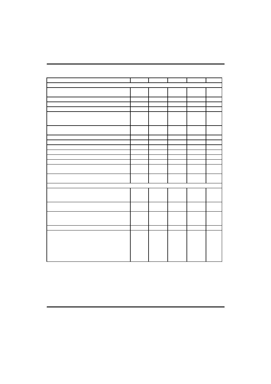
ELECTRICAL CHARACTERISTICS (
Ta=25
∞C, unless otherwise specified)
PARAMETER SYMBOL
MIN
TYP
MAX
UNIT
DC CHARACTERISTICS
Regulation Voltage
(Determined by external resistor divider)
V
Reg
14.85 V
Regulation Voltage Temperature Coefficient
Tc
-13
-11
-9.0
mV/
∞C
Suggested Battery Voltage Operating Range
Vbat
11.5
14.85
16.5
V
Power Up/Down Threshold Voltage (Pin 3)
Vpwr
0.5
1.2
2.0
V
Standby Current,
Vbat = 12.8 V, Ignition off, Ta = 25
∞C
Vbat = 12.8 V, Ignition off, -40
∞CTa125∞C
I
Q1
I
Q2
1.3
2.0
3.0
mA
mA
Zero Temperature Coefficient Reference Voltage,
(Pin 8)
Vref0 1.1 1.25 1.4 V
Band Gap Reference Voltage [Pin 20 (24**)]
Vref
1.7
2.0
2.3
V
Band Gap Reference Temperature Coefficient
TC
-13
-11
-9.0
mV/
∞C
Sense Loss Threshold (Pin 2)
S
Loss(th)
0.6 1.0 V
Phase Detection Threshold Voltage (Pin 10)
P
Th
1.0 1.25 1.5 V
Phase Rotation Detection Frequency (Pin 10)
P
Rot
36 Hz
Undervoltage Threshold [Pin 19 (23**)]
V
UV
1.0 1.25 1.5 V
Overvoltage Threshold
(Pin 2, or Pin 12 if Pin 2 is not used)
V
OV
1.09(Vref)
1.12(Vref)
1.16(Vref) V
Load Dump Threshold
(Pin 2, or Pin 12 if Pin 2 is not used)
V
LD
1.33(Vref)
1.4(Vref)
1.48(Vref) V
SWITCHING CHARACTERISTICS
Fundamental Regulation Output Frequency,
[Pin 17 (21**)]
(Clock oscillator frequency divided by 4096)
f 68 Hz
Suggested Clock Oscillator Frequency Range, (Pin 9)
(Determined by external resistor, RT)
fosc 205 280 350 kHz
Duty Cycle [Pin 17 (21**)]
At Start≠up
During Overvoltage Condition
Start
DC
OV
DC
27
3.5
29
4.7
31
5.5
%
Low/High RPM Transition Frequency (Pin 10)
LRC
Freq
247 273 309 Hz
LRC Duty Cycle Increase Rate
Low RPM Mode (LRCFreq < 247 Hz),
Pin 11 = Open (Slow Rat)
LRC
S
8.5
9.5 10.5
Low RPM Mode (LRCFreq < 247 Hz),
Pin 11 = Grounded (Fast Rate)
LRC
F
34 38 42
High RPM Mode (LRCFreq > 309 Hz),
Pin 11 = Don't Care (LRC Mode is disabled)
LRC
H
409 455 501
%/sec
NOTE: **
For 24-pin package.