
UTC LM2937-XX
LINEAR INTEGRATED CIRCUIT
UTC
UNISONIC TECHNOLOGIES CO., LTD.
1
QW-R102-012,C
500mA LOW DROPOUT VOLTAGE
REGULATOR
DESCRIPTION
The UTC LM2937-XX is a positive voltage regulator
capable of supplying up to 500mA of load current. The use of
a PNP power transistor provides a low dropout voltage
characteristic. With a load current of 500mA the minimum
input to output voltage differential required for the output to
remain in regulation is typically 0.5V(1V guaranteed maximum
over the full operating temperature range). Special circuitry
has been incorporated to minimize the quiescent current to
typically only 10mA with a full 500mA load current when the
input to output voltage differential is greater than 3V.
The UTC LM2937-XX requires an output bypass
capacitor for stability. As with most low dropout regulators, the
ESR of this capacitor remains a critical design parameter, but
the LM2937 includes special compensation circuitry that
relaxes ESR requirements. The UTC LM2937-XX is stable for
all ESR below 3.This allows the use of low ESR chip
capacitors.
Ideally suited for automotive applications, the UTC
LM2937-XX will protect itself and any load circuitry from
reverse battery connections, two-battery jumps and up to
+60V/-50V load dump transients. Familiar regulator features
such as short circuit and thermal shutdown protection are also
built in.
FEATURES
*Fully specified for operation over -40
�C to +125�C
*Output current in excess of 500mA
*Output trimmed for 5% tolerance under all operating
conditions
*Typical dropout voltage of 0.5V at full rated load current
*Wide output capacitor ESR range, up to 3
*Reverse battery protection
*Internal short circuit and thermal overload protection
*60V input transient protection
*Mirror image insertion protection
*Built-in ON/OFF control function
T0-220
1
T0-263
1
1
TO-263-5
TO-220/TO263 : 1:Input 2:GND 3:Output
TO-263-5 : 1: N/C 2: ON/OFF 3: GND
4: Input 5: Output

UTC LM2937-XX
LINEAR INTEGRATED CIRCUIT
UTC
UNISONIC TECHNOLOGIES CO., LTD.
2
QW-R102-012,C
TYPICAL APPLICATION
U N R E G U L A T E D
V
IN
C in *
1 0
F
V
O U T
L M 2 9 3 7 -X X
R E G U L A T E D
IN P U T
O U T P U T
C
O U T
* *
1 0
F
I
Q
1
2
3
ON/OFF CONTROL APPLICATION
U N R E G U L A T E D
V
IN
C in *
1 0
F
V
O U T
L M 2 9 3 7 -X X
R E G U L A T E D
IN P U T
O U T P U T
C
O U T
* *
1 0
F
I
Q
N /C
O N /O F F
4
1
3
2
5
* Required if the regulator is located more than 3 inches from the power supply filter capacitors.
**Required for stability. C
OUT
must be at least 10�F(over the full expected operating temperature range) and located
as close as possible to the regulator. The equivalent series resistance, ESR ,of this capacitor may be as high as
3.
ABSOLUTE MAXIMUM RATINGS(Note 1)
PARAMETER SYMBOL RATING
UNIT
Internal Power Dissipation(Note 2)
Internally limited
Input Voltage
V
IN
26
V
Storage temperature Range
Tstg
-65 ~ +150
�C
Maximum Junction Temperature
Tj
150
�C
LM2937-3.3V ELECTRICAL CHARACTERISTICS
( V
IN
=V
NOM
+5V,I
O
=500mA,C
out
=10�F, Tj=T
A
=25
�C ,unless otherwise specified )
PARAMETER SYMBOL
TEST
CONDITIONS
MIN.
TYP.
MAX.
UNIT.
Output Voltage
V
o
5mAI
O
500mA
3.21 3.30 3.39 V
Line Regulation
V
O
Vo+2VV
IN
26V, I
O
=5mA
9
30
mV
Load Regulation
V
O
5mAI
O
500mA
3
30
mV
(Vo+2V)V
IN
26V,I
O
=5mA 2
10
mA
Quiescent Current
I
Q
V
IN
= Vo+5V, I
O
=500mA
10
20
mA
Output Noise Voltage
V
NOISE
10Hz-100kHz,
I
O
=5mA
100
�Vrms
Long Term Stability
1000Hrs
12
mV

UTC LM2937-XX
LINEAR INTEGRATED CIRCUIT
UTC
UNISONIC TECHNOLOGIES CO., LTD.
3
QW-R102-012,C
PARAMETER SYMBOL
TEST
CONDITIONS
MIN.
TYP.
MAX.
UNIT.
I
O
=500mA
0.5
1.0
V
Dropout Voltage
V
D
I
O
=50mA
110
250
mV
Short Circuit Current
I
S
0.6 1.0
A
Peak Line Transient Voltage
T
in
tf100ms ,R
L
=100 60
75
V
Reverse DC Input Voltage
V
Rin
V
O
-0.6V ,R
L
=100
-15 -30
V
Reverse Transient Input
Voltage
V
TRRI
tf<1ms
,R
L
=100
-50
-75
V
LM2937-5.0V ELECTRICAL CHARACTERISTICS
(V
IN
=V
NOM
+5V,I
O
=500mA,C
out
=10�F, Tj=T
A
=25
�C,,unless otherwise specified )
PARAMETER SYMBOL
TEST
CONDITIONS
MIN.
TYP.
MAX.
UNIT.
Output Voltage
V
o
5mAI
O
500mA
4.85 5.00 5.15 V
Line Regulation
V
O
Vo+2VV
IN
26V, I
O
=5mA
15
50
mV
Load Regulation
V
O
5mAI
O
500mA
5
50
mV
(Vo+2V)V
IN
26V,I
O
=5mA 2
10
mA
Quiescent Current
I
Q
V
IN
= Vo+5V, I
O
=500mA
10
20
mA
Output Noise Voltage
V
NOISE
10Hz-100kHz,
I
O
=5mA
150
�Vrms
Long Term Stability
1000Hrs
20
mV
I
O
=500mA
0.5
1.0
V
Dropout Voltage
V
D
I
O
=50mA
110
250
mV
Short Circuit Current
I
S
0.6 1.0
A
Peak Line Transient Voltage
T
in
tf100ms ,R
L
=100 60
75
V
Reverse DC Input Voltage
V
Rin
V
O
-0.6V ,R
L
=100
-15 -30
V
Reverse Transient Input
Voltage
V
TRRI
tf<1ms
,R
L
=100
-50
-75
V
LM2937-8.0V ELECTRICAL CHARACTERISTICS
(V
IN
=V
NOM
+5V,I
O
=500mA,C
out
=10�F, Tj=T
A
=25
�C,,unless otherwise specified )
PARAMETER SYMBOL
TEST
CONDITIONS
MIN.
TYP.
MAX.
UNIT.
Output Voltage
V
o
5mAI
O
500mA
7.76 8.00 8.24 V
Line Regulation
V
O
Vo+2VV
IN
26V, I
O
=5mA
24
80
mV
Load Regulation
V
O
5mAI
O
500mA
8
80
mV
(Vo+2V)V
IN
26V,I
O
=5mA 2
10
mA
Quiescent Current
I
Q
V
IN
= Vo+5V, I
O
=500mA
10
20
mA
Output Noise Voltage
V
NOISE
10Hz-100kHz,
I
O
=5mA
240
�Vrms
Long Term Stability
1000Hrs
32
mV
I
O
=500mA
0.5
1.0
V
Dropout Voltage
V
D
I
O
=50mA
110
250
mV
Short Circuit Current
I
S
0.6 1.0
A
Peak Line Transient Voltage
T
in
tf100ms ,R
L
=100 60
75
V
Reverse DC Input Voltage
V
Rin
V
O
-0.6V ,R
L
=100
-15 -30
V
Reverse Transient Input
Voltage
V
TRRI
tf<1ms
,R
L
=100
-50
-75
V
LM2937-10.0V ELECTRICAL CHARACTERISTICS
(V
IN
=V
NOM
+5V,I
O
=500mA,C
out
=10�F, Tj=T
A
=25
�C,,unless otherwise specified )
PARAMETER SYMBOL
TEST
CONDITIONS
MIN.
TYP.
MAX.
UNIT.
Output Voltage
V
o
5mAI
O
500mA 9.70
10.00
10.30
V
Line Regulation
V
O
Vo+2VV
IN
26V, I
O
=5mA
30
100
mV
UTC LM2937-XX
LINEAR INTEGRATED CIRCUIT
UTC
UNISONIC TECHNOLOGIES CO., LTD.
4
QW-R102-012,C
PARAMETER SYMBOL
TEST
CONDITIONS
MIN.
TYP.
MAX.
UNIT.
Load Regulation
V
O
5mAI
O
500mA
10
100
mV
(Vo+2V)V
IN
26V,I
O
=5mA 2
10
mA
Quiescent Current
I
Q
V
IN
= Vo+5V, I
O
=500mA
10
20
mA
Output Noise Voltage
V
NOISE
10Hz-100kHz,
I
O
=5mA
300
�Vrms
Long Term Stability
1000Hrs
40
mV
I
O
=500mA
0.5
1.0
V
Dropout Voltage
V
D
I
O
=50mA
110
250
mV
Short Circuit Current
I
S
0.6 1.0
A
Peak Line Transient Voltage
T
in
tf100ms ,R
L
=100 60
75
V
Reverse DC Input Voltage
V
Rin
V
O
-0.6V ,R
L
=100
-15 -30
V
Reverse Transient Input
Voltage
V
TRRI
tf<1ms
,R
L
=100
-50
-75
V
LM2937-12.0V ELECTRICAL CHARACTERISTICS
(V
IN
=V
NOM
+5V,I
O
=500mA,C
out
=10�F, Tj=T
A
=25
�C,,unless otherwise specified )
PARAMETER SYMBOL
TEST
CONDITIONS
MIN.
TYP.
MAX.
UNIT.
Output Voltage
V
o
5mAI
O
500mA
11.64 12.00 12.36 V
Line Regulation
V
O
Vo+2VV
IN
26V, I
O
=5mA
36
120
mV
Load Regulation
V
O
5mAI
O
500mA
12
120
mV
(Vo+2V)V
IN
26V,I
O
=5mA 2
10
mA
Quiescent Current
I
Q
V
IN
= Vo+5V, I
O
=500mA
10
20
mA
Output Noise Voltage
V
NOISE
10Hz-100kHz,
I
O
=5mA
360
�Vrms
Long Term Stability
1000Hrs
44
mV
I
O
=500mA
0.5
1.0
V
Dropout Voltage
V
D
I
O
=50mA
110
250
mV
Short Circuit Current
I
S
0.6 1.0
A
Peak Line Transient Voltage
T
in
tf100ms ,R
L
=100 60
75
V
Reverse DC Input Voltage
V
Rin
V
O
-0.6V ,R
L
=100
-15 -30
V
Reverse Transient Input
Voltage
V
TRRI
tf<1ms
,R
L
=100
-50
-75
V
LM2937-15.0V ELECTRICAL CHARACTERISTICS
(V
IN
=V
NOM
+5V,I
O
=500mA,C
out
=10�F, Tj=T
A
=25
�C,,unless otherwise specified )
PARAMETER SYMBOL
TEST
CONDITIONS
MIN.
TYP.
MAX.
UNIT.
Output Voltage
V
o
5mAI
O
500mA
14.55 15.00 15.45 V
Line Regulation
V
O
Vo+2VV
IN
26V, I
O
=5mA
45
150
mV
Load Regulation
V
O
5mAI
O
500mA
15
150
mV
(Vo+2V)V
IN
26V,I
O
=5mA 2
10
mA
Quiescent Current
I
Q
V
IN
= Vo+5V, I
O
=500mA
10
20
mA
Output Noise Voltage
V
NOISE
10Hz-100kHz,
I
O
=5mA
450
�Vrms
Long Term Stability
1000Hrs
56
mV
I
O
=500mA
0.5
1.0
V
Dropout Voltage
V
D
I
O
=50mA
110
250
mV
Short Circuit Current
I
S
0.6 1.0
A
Peak Line Transient Voltage
T
in
tf100ms ,R
L
=100 60
75
V
Reverse DC Input Voltage
V
Rin
V
O
-0.6V ,R
L
=100
-15 -30
V
Reverse Transient Input
Voltage
V
TRRI
tf<1ms
,R
L
=100
-50
-75
V
UTC LM2937-XX
LINEAR INTEGRATED CIRCUIT
UTC
UNISONIC TECHNOLOGIES CO., LTD.
5
QW-R102-012,C
ON/OFF CONTROL
PARAMETER SYMBOL
TEST
CONDITIONS
MIN.
TYP.
MAX.
UNIT.
ON/OFF Threshold Voltage
ON
V
ON
I
O
0.5A
0.8
V
ON/OFF Threshold Voltage
OFF
V
OFF
I
O
0.5A
2.0
V
ON/OFF Threshold Current
I
ON/OFF
V
ON/OFF=
2.0V,Io=0.5A
50
100
A
Note 1: Absolute Maximum Ratings indicate limits beyond which damage to the device may occur. Electrical
Specifications do not apply when operating the device outside of its rated Operating Conditions.
Note 2: The maximum allowable power dissipation at any ambient temperature is P
MAX
=(125-T
A
)/
JA
, where 125 is
the maximum junction temperature for operation, T
A
is the ambient temperature, and
JA
is the junction to
ambient thermal resistance. If this dissipation is exceeded, the die temperature will rise above 125
�C and
the electrical specifications do not apply. If the die temperature rises above 150
�C, the LM2937 will go into
thermal shutdown. For the LM2937, the junction to ambient thermal resistance JA is 65
�C/W, for the
TO-220 package and 73
�C/W for the TO-263 package. When used with a heat sink,
JA
is the sum of the
LM2937 junction to case thermal resistance
JC
of 3
�C/W and the heat sink case to ambient thermal
resistance. If the TO-263packag is used, the thermal resistance can be reduced by increasing P.C. board
copper area thermally connected to the package.

UTC LM2937-XX
LINEAR INTEGRATED CIRCUIT
UTC
UNISONIC TECHNOLOGIES CO., LTD.
6
QW-R102-012,C
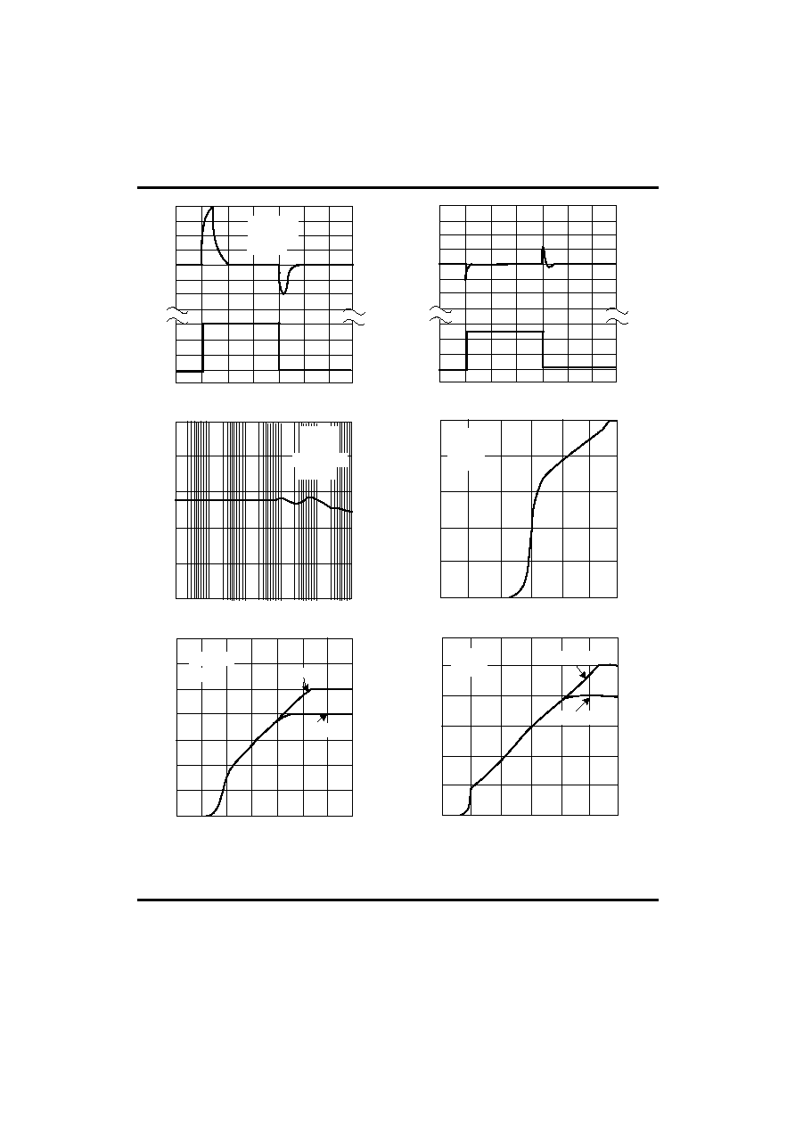
TYPICAL PERFORMANCE CHARACTERISTICS
0
200
0.4
Output Current (mA)
Dropout Voltage vs Output Current
D
r
op
ou
t
V
o
lt
ag
e (
V
)
300
0.2
0.3
0.5
0.1
100
400
500
0
0.6
0.7
0.8
0.9
Tj=25
-40
40
0.4
Dropout Voltage vsTemperature
D
r
o
p
ou
t
V
o
lt
ag
e (
V
)
80
0.2
0.3
0.5
0.1
0
120
0
0.6
0.7
0.8
0.9
0.5A
1.0
Temperature
()
0.25A
0.05A
-40
40
4.98
Output Voltage vs Temperature
O
u
t
p
u
t
V
o
lt
ag
e (
V
)
80
4.94
4.96
5.00
4.92
0
120
4.90
5.02
5.04
5.06
5.08
5.10
Temperature
()
-40
40
10
Quiescent Current vs Temperature
Q
u
i
e
s
c
e
n
t
C
u
rre
n
t
(m
A
)
80
5
0
120
0
15
20
Temperature
()
250mA
500mA
5mA
R
L
=100
0
10
20
Quiescent Current vs Input Voltage
Q
u
i
e
s
c
e
n
t
C
u
rr
e
n
t
(m
A
)
15
10
5
20
25
0
30
40
50
Input Voltage (V)
0.25A
0.05A
30
35
60
70
80
90
100
0.5A
0
200
4
Q
u
i
e
s
c
e
n
t
C
u
rre
n
t
(m
A
)
300
1
100
400
500
0
6
8
10
Output Current (mA)
V
IN
=14V
V
O
=5V
Tj=25
V
O
=5V
T
A
=25
Quiescent Current vs Input Voltage
2
5
3
7
9
UTC LM2937-XX
LINEAR INTEGRATED CIRCUIT
UTC
UNISONIC TECHNOLOGIES CO., LTD.
7
QW-R102-012,C
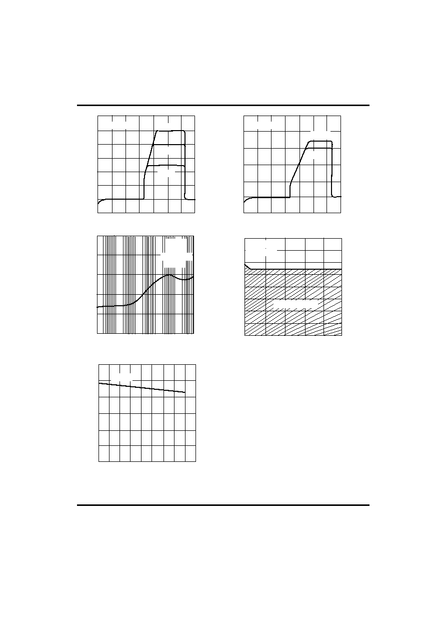
-10
10
Line Transient Response
20
-20
0
3V
0
30
40
0V
20
40
100
Ripple Rejection
R
i
p
p
le R
e
j
e
c
t
ion
(
d
B
)
1K
40
50
10
10K
100K
60
70
Frequency (Hz)
1.0
3.0
Low Voltage Behavior
O
u
t
p
u
t
V
o
lt
ag
e (
V
)
4.0
2.0
2.0
5.0
6.0
1.0
3.0
4.0
5.0
Input Voltage (V)
0
4
6
2
2
8
10
0
4
6
Input Voltage (V)
12
14
8
10
12
14
50
60
Load Transient Response
Lo
a
d
Cu
r
r
e
n
t
(
A
)
I
OUT
=50mA
Vo=5 V
T
A
=25
Time (
s)
1M
Io=500mA
Vo=5 V
Tj=25
O
u
tp
u
t
V
o
l
t
ag
e (
V
)
Low Voltage Behavior
Io=500mA
Tj=25
0
6
3
3
9
12
0
6
Input Voltage (V)
15
18
9
12
15
18
O
u
tp
u
t
V
o
l
t
ag
e (
V
)
Low Voltage Behavior
Vo=15 V
Tj=25
In
p
u
t V
o
l
t
ag
e
C
h
a
nge
(
V
)
O
u
tp
u
t
V
o
l
t
a
g
e
De
v
i
a
t
i
o
n
(
m
V
)
Time (
s)
-1
1
2
-50
0
400
0
3
4
0
50
5
6
O
u
tp
u
t
V
o
l
t
a
g
e
De
v
i
a
t
i
o
n
(
m
V
)
V
IN
=10V
Vo=5 V
Io=50mA
C
OUT
=10 F
0
0
Vo=10V
Vo=8 V
Io=500mA
Vo=12 V
UTC LM2937-XX
LINEAR INTEGRATED CIRCUIT
UTC
UNISONIC TECHNOLOGIES CO., LTD.
8
QW-R102-012,C
Output Impedance
0
200
100
300
0.01
0.1
1
Output Current (mA)
400
500
10
100
E
quiv
a
lent
S
e
r
i
es
R
e
s
i
s
t
an
c
e
(
)
Output Capacitor ESR
Vo=5V
-30
-10
0
0
-20
10
20
-2
2
6
Input Voltage (V)
30
40
8
10
12
O
u
tput
V
o
lt
ag
e
(V
)
Output at Voltage Extremes
R
L
=100
Vo=10V
-30
-10
0
0
-20
10
20
-4
4
8
Input Voltage (V)
30
40
12
16
20
O
u
tput
V
o
lt
ag
e
(V
)
Output at Voltage Extremes
R
L
=100
Vo=12V
C
OUT
=10
F
-40
0
40
80
0
0.5
Temperature (
)
120
1.0
1.5
O
u
tput C
u
r
r
ent (A
)
Peak Output Current
V
IN
=14V
O
u
tput I
m
pe
danc
e (
)
4
Vo=8V
Vo=5V
Vo=15V
100
1K
0.01
0.1
10
10K
100K
1.0
10
Frequency (Hz)
1M
V
IN
=14V
Vo=5 V
Io=25mA
C
OUT
=10
F
STABLE REGION