
UTC MC14511
CMOS IC
UTC
UNISONIC TECHNOLOGIES CO., LTD.
1
QW-R502-021,B
BCD-TO-SEVEN SEGMENT
LATCH/DECODER/DRIVER
DESCRIPTION
The UTC MC14511 BCD≠to≠seven segment
latch/decoder/driver is constructed with complementary
MOS (CMOS) enhancement mode devices and NPN
bipolar output drivers in a single monolithic structure. The
circuit provides the functions of a 4-bit storage latch, an
8421 BCD-to-seven segment decoder, and an output
drive capability. Lamp test (LT), blanking (BI), and latch
enable (LE) inputs are used to test the display, to turn-off
or pulse modulate the brightness of the display, and to
store a BCD code, respectively. It can be used with
seven-segment light-emitting diodes (LED),
incandescent, fluorescent, gas discharge, or liquid crystal
readouts either directly or indirectly.
Applications include instrument (e.g., counter, DVM,
etc.) display driver, computer/calculator display driver,
cockpit display driver, and various clock, watch, and
timer uses.
FEATURES
* Low Logic Circuit Power Dissipation
* High≠Current Sourcing Outputs (Up to 25 mA)
* Latch Storage of Code
* Blanking Input
* Lamp Test Provision
* Readout Blanking on all Illegal Input Combinations
* Lamp Intensity Modulation Capability
* Time Share (Multiplexing) Facility
* Supply Voltage Range = 3.0 V ~ 18 V
* Capable of Driving Two Low-power TTL Loads, One
Low-power Schottky TTL Load or Two HTL Loads Over
the Rated Temperature Range
* Chip Complexity: 216 FETs or 54 Equivalent Gates
* Triple Diode Protection on all Inputs
DIP-16
SOP-16

UTC MC14511
CMOS IC
UTC
UNISONIC TECHNOLOGIES CO., LTD.
2
QW-R502-021,B
PIN CONFIGURATION
0
1
2
3
4
5
6
7
8
9
DISPLAY
B
C
LT
BI
LE
D
A
Vss
e
d
c
b
a
g
f
V
DD
1
2
3
4
5
6
7
8
16
15
14
13
12
11
10
9
g
a
b
f
d
e
c
TRUTH TABLE
Inputs Outputs
LE
BI
LT
D C B A
a
b
c
d
e
f
g
Display
X
X
0
X X X X
1
1
1
1
1
1
1
8
X
0
1
X X X X
0
0
0
0
0
0
0
Blank
0
0
0
0
1
1
1
1
1
1
1
1
0 0 0 0
0 0 0 1
0 0 1 0
0 0 1 1
1
0
1
1
1
1
1
1
1
1
0
1
1
0
1
1
1
0
1
0
1
0
0
0
0
0
1
1
0
1
2
3
0
0
0
0
1
1
1
1
1
1
1
1
0 1 0 0
0 1 0 1
0 1 1 0
0 1 1 1
0
1
0
1
1
0
0
1
1
1
1
1
0
1
1
0
0
0
1
0
1
1
1
0
1
1
1
0
4
5
6
7
0
0
0
0
1
1
1
1
1
1
1
1
1 0 0 0
1 0 0 1
1 0 1 0
1 0 1 1
1
1
0
0
1
1
0
0
1
1
0
0
1
0
0
0
1
0
0
0
1
1
0
0
1
1
0
0
8
9
Blank
Blank
0
0
0
0
1
1
1
1
1
1
1
1
1 1 0 0
1 1 0 1
1 1 1 0
1 1 1 1
0
0
0
0
0
0
0
0
0
0
0
0
0
0
0
0
0
0
0
0
0
0
0
0
0
0
0
0
Blank
Blank
Blank
Blank
1
1
1
X X X X
*
*
X=Don't Care
*Depends upon the BCD code previously applied when LE=0
UTC MC14511
CMOS IC
UTC
UNISONIC TECHNOLOGIES CO., LTD.
3
QW-R502-021,B
This device contains protection circuitry to protect the inputs against damage due to high static voltages or electric
fields. However, it is advised that normal precautions be taken to avoid application of any voltage higher than
maximum rated voltages to this high-impedance circuit. A destructive high current mode may occur if V
in
and V
out
are
not constrained to the range:
V
SS
(V
in
or V
out
) V
DD
.
Due to the sourcing capability of this circuit, damage can occur to the device if V
DD
is applied, and the outputs are
shorted to V
SS
and are at a logical 1 (See Maximum Ratings).
Unused inputs must always be tied to an appropriate logic voltage level (e.g., either V
SS
or V
DD
).
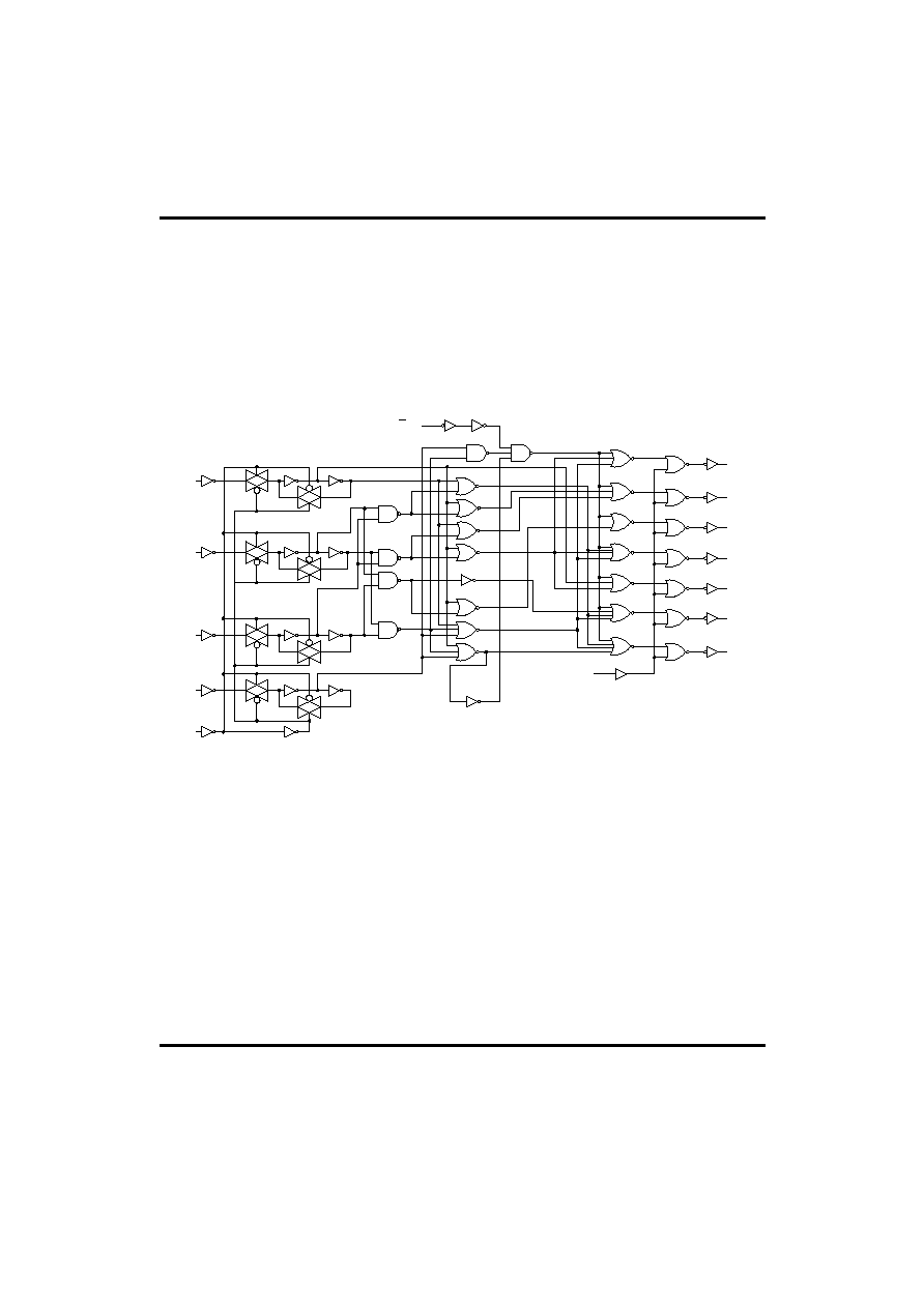
BLOCK DIAGRAM
LE 5
D 6
C 2
B
1
A
7
V
DD
=PIN 16
V
ss
=PIN 8
14 g
15 f
9 e
10 d
11 c
12 b
13 a
BI 4
LT 3

UTC MC14511
CMOS IC
UTC
UNISONIC TECHNOLOGIES CO., LTD.
4
QW-R502-021,B
ABSOLUTE MAXIMUM RATINGS
(Voltages Referenced to Vss) (Note 1)
PARAMETER SYMBOL RATINGS
UNIT
DC Supply Voltage Range
V
DD
-0.5 ~ +18.0
V
Input Voltage Range, All Inputs
Vin
-0.5 ~ V
DD
+0.5 V
DC Current Drain per Input Pin
I
10
mA
Power Dissipation, per Package
(Note 2)
P
D
500
mW
Maximum Output Drive Current
(Source) per Output
I
OHmax
25
mA
Maximum Continuous Output
Power (Source) per Output (Note 3)
P
OHmax
50
mA
Operating Temperature Range
T
a
-55 ~ +125
Storage Temperature Range
Tstg
-65 ~ +150
Note 1: Maximum Ratings are those values beyond which damage to the device may occur.
Note 2: Temperature Derating:
Plastic "P and D/DW" Packages: - 7.0 mW/ From 65 ~ 125
Note 3: P
OHmax
= I
OH
(V
DD
≠ V
OH
)
ELECTRICAL CHARACTERISTICS
(Voltages Referenced to Vss)
PARAMETER SYMBOL
V
DD
Vdc
TEST CONDITIONS
MIN
TYP
MAX
UNIT
V
OL
5.0
10
15
"0" Level
Vin=V
DD
or 0
0
0
0
0.05
0.05
0.05
V
Output Voltage
V
OH
5.0
10
15
"1" Level
Vin=0 or V
DD
4.1
9.1
14.1
4.57
9.58
14.59
V
V
IL
5.0
10
15
"0" Level
Vo=3.8 or 0.5 V
Vo=8.8 or 1.0 V
Vo=13.8 or 1.5V
2.25
4.50
6.75
1.5
3.0
4.0
V
Input Voltage #
V
IH
5.0
10
15
"1" Level
Vo=0.5 or 3.8 V
Vo=1.0 or 8.8 V
Vo=1.5 or 13.8 V
3.5
7.0
11
2.75
5.50
8.25
V
5.0 I
OH
=0mA Source
I
OH
=5.0mA
I
OH
=10mA
I
OH
=15mA
I
OH
=20mA
I
OH
=25mA
4.1
3.9
3.4
4.57
4.24
4.12
3.94
3.70
3.54
V
Output Drive Voltage
V
OH
10 I
OH
=0mA Source
I
OH
=5.0mA
I
OH
=10mA
I
OH
=15mA
I
OH
=20mA
I
OH
=25mA
9.1
9.0
8.6
9.58
9.26
9.17
9.04
8.90
8.70
V

UTC MC14511
CMOS IC
UTC
UNISONIC TECHNOLOGIES CO., LTD.
5
QW-R502-021,B
PARAMETER SYMBOL
V
DD
Vdc
TEST CONDITIONS
MIN
TYP
MAX
UNIT
Output Drive Voltage
V
OH
15 I
OH
=0mA Source
I
OH
=5.0mA
I
OH
=10mA
I
OH
=15mA
I
OH
=20mA
I
OH
=25mA
14.1
14
13.6
14.59
14.27
14.18
14.07
13.95
13.70
V
Output Drive Current
I
OL
5.0
10
15
V
OL
=0.4V Sink
V
OL
=0.5V
V
OL
=1.5V
0.51
1.3
3.4
0.88
2.25
8.8
mA
Input Current
I
in
15
±0.00001
±
0.1
A
Input Capacitance
C
in
5.0 7.5 pF
Quiescent Current
I
DD
5.0
10
15
(Per Package) Vin=0 or
V
DD,
Iout=0A
0.005
0.010
0.015
5.0
10
20
A
Total Supply Current
(Notes 5 & 6)
I
T
5.0
10
15
(Dynamic plus Quiescent,
Per Package)
(C
L
=50pF on all outputs, all
buffers switching)
I
T
=(1.9A/kHz) f+I
DD
I
T
=(3.8A/kHz) f+I
DD
I
T
=(5.7A/kHz) f+I
DD
A
Note 4: Noise immunity specified for worst≠case input combination.
Noise Margin for both "1" and "0" level =
1.0 V min @ V
DD
= 5.0 V
2.0 V min @ V
DD
= 10 V
2.5 V min @ V
DD
= 15 V
Note 5: The formulas given are for the typical characteristics only at 25.
Note 6: To calculate total supply current at loads other than 50 pF:
I
T
(C
L
) = I
T
(50 pF) + 3.5 x 10
≠3
(C
L
≠ 50) V
DD
f
Where: I
T
is inA (per package), C
L
in pF, V
DD
in Vdc, and f in kHz is input frequency.