
UTC MCR106
SCR
UTC
UNISONIC TECHNOLOGIES CO., LTD.
1
QW-R301-001,A
REVERSE BLOCKING TRIODE
THYRISTORS
DESCRIPTION
PNPN devices designed for high volume consumer
applications such as temperature, light and speed
control; process and remote control, and warning
systems where reliability of operation is important.
FEATURES
*Glass-Passivated surface for reliability and
uniformity
*Power rated at economical prices
*Practical level triggering and holding characteristics
*Flat, rugged, thermopad construction for low thermal
resistance, high heat dissipation and durability
TO-126
1
1:CATHODE 2:ANODE 3:GATE
ABSOLUTE MAXIMUM RATINGS
(Tj=25
∞
C unless otherwise noted.)
PARAMETER SYMBOL
MAX
UNIT
Peak Repetitive Forward and Reverse Blocking Voltage (note 1)
(Tj=110
∞
C, R
GK
=1k
)
MCR106-6
MCR106-8
V
DRM
, V
RRM
400
600
V
RMS Forward Current (All conduction Angles)
I
T(RMS)
4
A
Average Forward Current (T
C
=93
∞
C or T
A
=30
∞
C)
I
T(AV)
2.55 A
Peak Non-repetitive Surge Current
(1/2 Cycle, 60Hz, Tj=-40 to +110
∞
C)
I
TSM
25 A
Circuit Fusing Considerations (t=8.3 ms)
I
2
t 2.6 A
2
Peak Gate Power
P
GM
0.5 W
Average Gate Power
P
G(AV)
0.1 W
Peak Forward Gate Current
I
GM
0.2 A
Peak Reversed Gate Voltage
V
RGM
6 V
Operating Junction Temperature Range
Tj
-40 ~ +110
∞
C
Storage Temperature Range
Tstg
-40 ~ +150
∞
C
Mounting Torque (note 2)
6
In. lb.
Note 1: V
DRM
and V
RRM
for all types can be applied on a continuous basis. Ratings apply for zero or negative gate
voltage; however, positive gate voltage shall not be applied concurrent with negative potential on the anode.
Blocking voltages shall not be tested with a constant current source such that the voltage of the devices are
exceeded.
UTC MCR106
SCR
UTC
UNISONIC TECHNOLOGIES CO., LTD.
2
QW-R301-001,A
Note 2: Torque rating applies with use of compression washer (B52200-F006 or equivalent). Mounting torque in
excess of 6 in. lb. does not appreciably lower case-to-sink thermal resistance. Anode lead and heatsink
contact pad are common. For soldering purposes (either terminal connection or device mounting), soldering
temperatures shall not exceed +200
∞
C. For optimum results, an activated flux (oxide removing) is
recommended.
THERMAL CHARACTERISTICS
PARAMETER SYMBOL
MAX
UNIT
Thermal Resistance, Junction to Case
R
JC
3
∞
C/W
Thermal Resistance, Junction to Ambient
R
JA
75
∞
C/W
ELECTRICAL CHARACTERISTICS
(Tc=25
∞
C and R
GK
=1000
unless otherwise stated)
PARAMETER SYMBOL
MIN
TYP
MAX
UNIT
Peak Forward or Reverse Blocking Current
(V
AK
=Rated V
DRM
or V
RRM
) Tj=25
∞
C
Tj=100
∞
C
I
DRM
,I
RRM
10
200
µ
A
µ
A
Forward "On" Voltage
(I
TM
=4A peak)
V
TM
2
V
Gate Trigger Current (continuous dc) (Note)
(V
AK
=7V, R
L
=100
)
(V
AK
=7V, R
L
=100
, Tc=-40
∞
C)
I
GT
200
500
µ
A
Gate Trigger Voltage (continuous dc)
(V
AK
=7V, R
L
=100
, Tc=25
∞
C)
V
GT
1
V
Gate Non-Trigger Voltage
(V
AK
=Rated V
DRM
, R
L
=100
, Tj=110
∞
C)
V
GD
0.2 V
Holding Current
(V
AK
=7V, Tc=25
∞
C)
I
H
5
mA
Forward Voltage Application Rate
(Tj=110
∞
C)
dv/dt 10 V/
µ
s
Note: R
GK
current is not included in measurement.
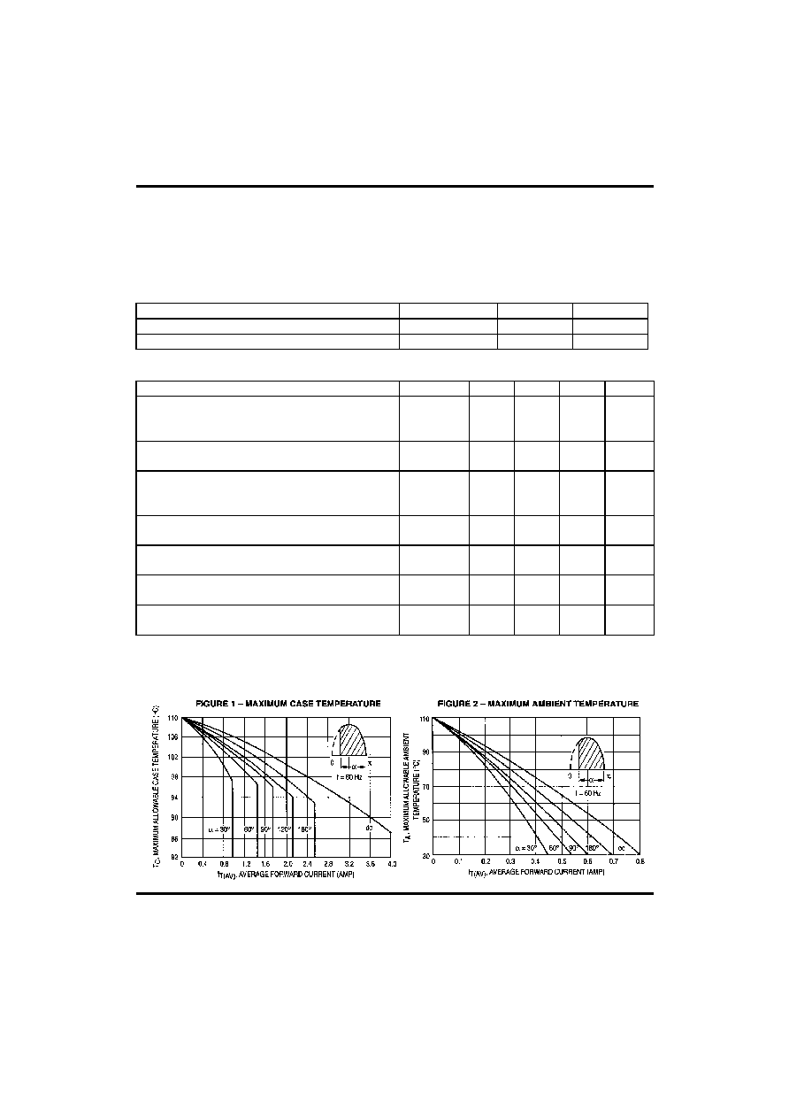
CURRENT DERATING