 | –≠–ª–µ–∫—Ç—Ä–æ–Ω–Ω—ã–π –∫–æ–º–ø–æ–Ω–µ–Ω—Ç: UTCTL5001 | –°–∫–∞—á–∞—Ç—å:  PDF PDF  ZIP ZIP |

UTC TL5001
LINEAR INTEGRATED CIRCUIT
UTC
UNISONIC TECHNOLOGIES CO., LTD.
1
QW-R103-016,A
PULSE-WIDTH-MODULATION
CONTROL CIRCUITS
DESCRIPTION
The UTC TL5001 incorporates on a single monolithic chip
all the functions required for a pulse-width ≠modulation
(PWM) control circuit. Designed primarily for power-supply
control, It contains an error amplifier, a regulator, an
oscillator, a PWM comparator with a dead-time-control input,
undervoltage lockout (UVLO),short-circuit
protection(SCP),and an open-collector output transistor.
The error-amplifier common-mode voltage ranges from 0V
to 1.5V. The noninverting input of the error amplifier is
connected to a 1-V reference. Dead-time control (DTC) can
be set to provide 0% to 100% dead time by connecting an
external resistor between DTC and GND. The oscillator
frequency is set by terminating RT with an external resistor to
GND. During low Vcc conditions, the UVLO circuit turns the
output off until Vcc recovers to its normal operating range.
FEATURES
*Complete PWM power control
*3.6-V to 40-V Operation
*Internal Undervoltage-Lockout Circuit
*Internal Short-Circuit Protection
*Oscillator Frequency : 20kHz to 500kHz
*Variable Dead Timer Provides Control Over Total Range
DIP-8
SOP-8

UTC TL5001
LINEAR INTEGRATED CIRCUIT
UTC
UNISONIC TECHNOLOGIES CO., LTD.
2
QW-R103-016,A
SCHEMATIC FOR TYPICAL APPLICATION
+
+
1
2
3
4
5
6
7
8
V
I
V
0
V
CC
SCP
DTC
RT
FB
COMP
V
0
UTC
TL5001
TSP1101
GND
FUNCTIONAL BLOCK DIAGRAM
1
2
3
4
5
6
7
8
UVLO
OSC
Reference
Voltage
I
DT
V
CC
DTC
RT
OUT
GND
PWM/DTC
Comparator
scp
Comparator 2
scp
Comparator 1
Error
Amplifier
SCP
FB
COMP
+
-
1V
1.5V
2.5V
1V
UTC TL5001
LINEAR INTEGRATED CIRCUIT
UTC
UNISONIC TECHNOLOGIES CO., LTD.
3
QW-R103-016,A
DETAILED DESCRIPTION
VOLTAGE REFERENCE
A 2.5-V regulator operating from Vcc is used to power the internal circuitry of the TL5001 and as a reference for the
error amplifier and SCP circuit. A resistive divider provides a 1-V reference for the error amplifier noninverting input
which typically is within 2% of nominal over the operating temperature range.
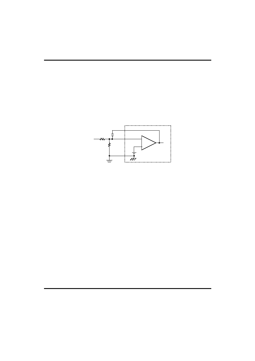
ERROR AMPLIFIER
The error amplifier compares a sample of the dc-to-dc converter output voltage to the 1-V reference and generates
an error signal for the PWM comparator. The dc-to-dc converter output voltage is set by selecting the error ≠amplifier
gain(see Figure 1),using the following expression.
Vo=(1+R1/R2) (1V)
+
-
FB
COMP
GND
V
I(FB)
R1
R2
Vref=1V
To PWM
Comparator
Compensation
Network
3
4
8
Figure 1.Error-Amplifier Gain Setting
The error-amplifier output is brought out as COMP for use in compensating the dc-to-dc converter control loop for
stability. Because the amplifier can only source 45µA,the total dc load resistance should be 100k or more.
OSCILLATOR/PWM
The oscillator frequency (fosc) can be set between 20kHz and 500kHz by connecting a resistor between RT and
GND .Acceptable resistor values range from 15 kto 250 kThe oscillator frequency can be determined by using
the graph shown in Figure 5.
The oscillator output is a triangular wave with a minimum value of approximately 0.7V and a maximum value of
approximately 1.3V. The PWM comparator compares the error-amplifier output voltage and the DTC input voltage to
the triangular wave and turns the output transistor off whenever the triangular wave is greater than the lesser of the
two inputs.
DEAD TIME CONTORL (DTC)
DTC provides a means of limiting the output ≠switch duty cycle to a value less than 100%, which is critical for boost
and flyback converters. A current source generates a reference current (I
DT
) at DTC that is nominally equal to the
current at the oscillator timing terminal, RT. Connecting a resistor between DTC and GND generates a dead-time
reference voltage (V
DT
), which the PWM/DTC comparator compares to the oscillator triangle wave as described in
the previous section. Nominally, the maximum duty cycle is 0% when V
DT
is 0.7V or less and 100% when V
DT
is
1.3V or greater. Because the triangle wave amplitude is a function of frequency and the source impedance of RT is
relatively high(1250),choosing R
DT
for a specific maximum duty cycle, D, is accomplished using the following
equation and the voltage limits for the frequency in question as found in Figure 11(Vosc
max
and Vosc
min
are the
maximum and minimum oscillator levels):
R
DT
=(Rt +1250)[D(Vosc
max
-Vosc
min
)+Vosc
min
]
Where
R
DT
and Rt are in ohms,D in decimal
UTC TL5001
LINEAR INTEGRATED CIRCUIT
UTC
UNISONIC TECHNOLOGIES CO., LTD.
4
QW-R103-016,A
Soft start can be implemented by paralleling the DTC resistor with a capacitor (C
DT
) as shown in Figure 2. During
soft start, the voltage at DTC is derived by the following equation:
V
DT
I
DT
R
DT
(1-e
(-t/R
DT
C
DT
)
)
UTC
TL5001
R
DT
C
DT
DTC
6
Figure 2. Soft- Start Circuit
If the dc-to-dc converter must be in regulation within a specified period of time, the time constant , R
DT
C
DT
, should
be t0/3 to t0/5.The TL5001 remains off unit V
DT
0.7V,the minimum ramp value. C
DT
is discharged every time UVLO
or SCP becomes active.
UNDERVOLTAGE-LOCKOUT (UVLO) PROTECTION
The undervoltage-lockout circuit turns the output transistor off and resets the SCP latch whenever the supply voltage
drops too low (approximately 3V at 25) for proper operation. A hysteresis voltage of 200mV eliminates false
triggering on noise and chattering.
SHORT-CIRCUIT PROTECTION (SCP)
The TL5001 includes short-circuit protection (see Figure 3),which turns the power switch off to prevent damage
when the converter output is shorted. When activated, The SCP prevents the switch from being turned on until the
internal latching circuit is reset. The circuit is reset by reducing the input voltage until UVLO becomes active or until
the SCP terminal is pulled to ground externally.
When a short circuit occurs, the error-amplifier output at COMP rises to increase the power-switch duty cycle in an
attempt to maintain the output voltage. SCP comparator 1 starts an RC timing circuit when COMP exceeds 1.5V.If
the short is removed and the error-amplifier output drops below 1.5V before time out, normal converter operation
continues. If the fault is still present at the end of the time-out period, the time sets the latching circuit and turns off
the TL5001 output transistor.
2.5V
R
SCP
185k
12k
C
SCP
SCP
From Error Amp
1.5V
scp
Comparator 1
Q2
Q1
Vref=1V
scp
Comparator 2
To Output
Drive Logic
Figure 3.SCP Circuit
5
UTC TL5001
LINEAR INTEGRATED CIRCUIT
UTC
UNISONIC TECHNOLOGIES CO., LTD.
5
QW-R103-016,A
The timer operates by charging an external capacitor (Cscp),connected between the SCP terminal and ground,
towards 2.5V through a 185k
resistor (Rscp).The circuit begins charging from an initial voltage of approximately
185mV and times out when capacitor voltage reaches 1V.The output of SCP comparator 2 then goes high, turns on
Q2,and latches the timer circuit. The expression for setting the SCP time period is derived from the following
equation:
Vscp =(2.5-0.185)(1-e
-t/
)+0.185
Where
=RscpCscp
The end of the time-out period, tscp, occurs when Vscp=1V. Solving for Cscp yields:
Cscp=12.46*tscp
Where
t is in seconds,C in µF
tscp must be much longer (generally 10 to 15 times) than the converter start-up period or the converter will not start.
OUTPUT TRANSISTOR
The output of the TL5001 is an open-collector transistor with a maximum collector current rating of 21mA and a
voltage rating of 51V.The output is turned on under the following conditions: the oscillator triangle wave is lower than
both the DTC voltage and the error-amplifier output voltage, the UVLO circuit is inactive, and the short-circuit
protection circuit is inactive.
ABSOLUTE MAXIMUM RATINGS OVER OPERATING FREE-AIR TEMPERATURE
RANGE
(unless otherwise noted)*
PARAMETER SYMBOL
VALUE
UNIT
Supply Voltage (note 1)
V
CC
41 V
Amplifier Input Voltage
V
I(FB)
20 V
Output Voltage
V
O
51 V
Output Current
I
O
21 mA
Output Peak Current
I
O(peak)
100 mA
Continuous Total Power Dissipation
See dissipation rating table
Operating Ambient Temperature Range
T
A
-20 to 85
∞
C
Storage Temperature Range
T
stg
-65 to 150
∞
C
Lead Temperature 1.6mm(1/16 inch) from
Case for 10 Seconds.
T
case
260
∞
C
Note 1: All voltage values are with respect to the network ground terminal.
*Stresses beyond those listed under" absolute maximum ratings" may cause permanent damage to the device.
These are stress ratings only, and functional operation of the device at these or any other conditions beyond those
indicated under" recommended operating conditions" is not implied. Exposure to absolute-maximum-rated conditions
for extended periods may affect device reliability.
DISSIPATION RATING TABLE
PACKAGE T
A
25
∞
C
POWER RATING
DERATING FACTOR
ABOVE T
A
=25
∞
C
T
A
=70
∞
C
POWER RATING
T
A
=70
∞
C
POWER RATING
T
A
=70
∞
C
POWER RATING
SOP-8 725mW
5.8mW/
∞
C
464mW 377mW 145mW
DIP-8 1000mW
8.0mW/
∞
C
640mW 520mW 200mW
UTC TL5001
LINEAR INTEGRATED CIRCUIT
UTC
UNISONIC TECHNOLOGIES CO., LTD.
6
QW-R103-016,A
RECOMMENDED OPERATING CONDITIONS
PARAMETER SYMBOL
MIN
MAX
UNIT
Supply Voltage
V
CC
3.6
40
V
Amplifier Input Voltage
V
I(FB)
0
1.5
V
Output Voltage
V
O,
OUT 50
V
Output Current
I
O,
OUT 20
mA
COMP Source Current
45
µ
A
COMP dc Load Resistance
100
k
Oscillator Timing resistor
Rt
15
250
k
Oscillator Frequency
fosc
20
500
kHz
Operating Ambient Temperature Range
T
A
-20
85
∞
C
ELECTRICAL CHARACTERISTICS OVER RECOMMENDED OPERATING FREE-AIR
TEMPERATURE RANGE (
Vcc=6V, fosc=100kHz, all typical values at T
A
=25
∞
C, unless otherwise noted)
PARAMETER
TEST CONDITIONS
MIN
TYP MAX UNIT
Reference
Output Voltage
COMP Connected to FB
0.95
1
1.05
V
Input Regulation
Vcc=3.6V to 40V
2
12.5
mV
T
A
= -20
∞
C to 25
∞
C
-10
-1 10
Output Voltage Change with Temperature
T
A
= 25
∞
C to 85
∞
C
-10
2 10
mV/V
Undervoltage Lockout
Upper Threshold Voltage
T
A
= 25
∞
C
3
V
Lower Threshold Voltage
T
A
= 25
∞
C
2.8
V
Hysteresis
T
A
= 25
∞
C
100
200
mV
Reset Threshold Voltage
T
A
= 25
∞
C
2.1
2.55
V
Short Circuit Protection
SCP Threshold voltage
T
A
= 25
∞
C
0.95
1.00
1.05
V
SCP Voltage, Latched
No pullup
140
185 230
mV
SCP voltage, UVLO Standby
No pullup
60
120
mV
Input Source Current
T
A
= 25
∞
C
-10
-15 -20
µ
A
SCP Comparator 1 Threshold Voltage
1.5
V
Oscillator
Frequency
R
t
=100k
100 kHz
Standard Deviation of Frequency
15
kHz
Frequency Change with Voltage
Vcc=3.6V to 40V
1
kHz
T
A
= -40
∞
C to 25
∞
C
-4 -0.4 4 kHz
T
A
= -20
∞
C to 25
∞
C
-4 -0.4 4 kHz
Frequency Change with Temperature
T
A
= 25
∞
C to 85
∞
C
-4 -0.2 4 kHz
Voltage at RT
1
V
Dead-time Control
Output (source) Current
V
(DT)
=1.5V 0.9*I
RT
(NOTE)
1.1*I
RT
(NOTE)
µ
A
Duty cycle=0%
0.5
0.7
Input Threshold Voltage
Duty cycle=100%
1.3
1.5
V
Error Amplifier
Input Voltage
Vcc=3.6V to 40V
0
1.5
V

UTC TL5001
LINEAR INTEGRATED CIRCUIT
UTC
UNISONIC TECHNOLOGIES CO., LTD.
7
QW-R103-016,A
PARAMETER
TEST CONDITIONS
MIN
TYP MAX UNIT
Input Bias Current
-160
-500
nA
Output Voltage Swing Positive
1.5
2.3
V
Negative
0.3
0.4
V
Open-loop Voltage Amplification
80
dB
Unity-gain
Bandwidth
1.5 MHz
Output (sink) Current
V
I(FB)
=1.2V, COMP=1V
100
600
µ
A
Output (source) Current
V
I(FB)
=0.8V, COMP=1V
-45
-70
µ
A
Output
Output Saturation Voltage
Io=10mA
1.5
2
V
Vo=50V,Vcc=0
10
Off-state Current
Vo=50V
10
µ
A
Short-circuit Output Current
Vo=6V
40
mA
Total Device
Standby Supply Current (Off state)
1
1.5
mA
Average Supply Current
R
t
=100k
1.4
2.1
mA
Note: Output source current at RT
OSC
V
CC
OUT
scp
Comparator 1
COMP
2.3V
1.5V
3V
1V
DTC
PWM/DTC
Comparator
scp
Comparator 2
scp
SCP Timing Period
0V
NOTE A:The waveforms show timing characteristics for an intermittent short circuit and a longer short circuit that is sufficient to activate SCP.
Figure 4. PWM Timing Diagram
PARAMETER MEASUREMENT INFORMATION
UTC TL5001
LINEAR INTEGRATED CIRCUIT
UTC
UNISONIC TECHNOLOGIES CO., LTD.
8
QW-R103-016,A
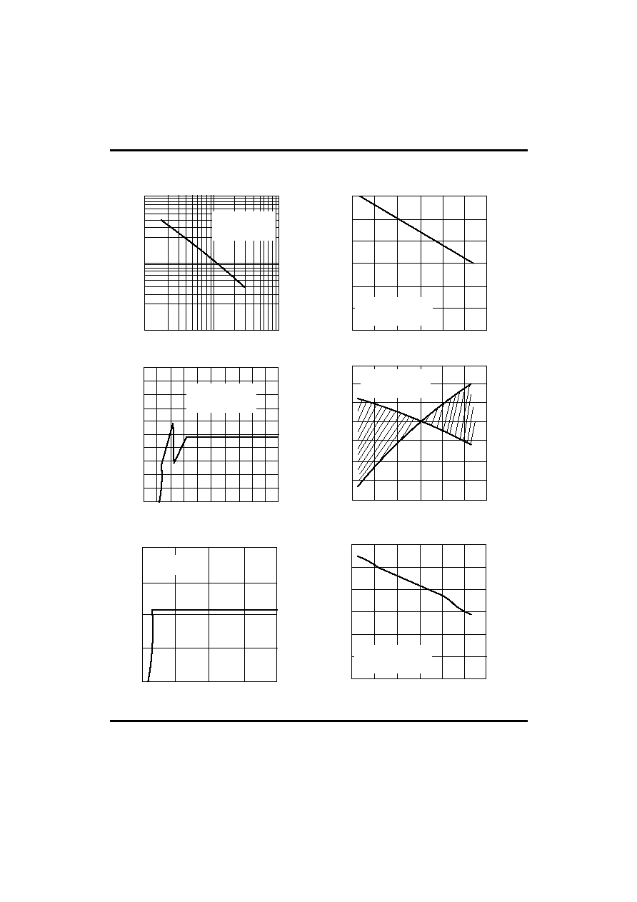
TYPICAL CHARACTERISTICS
-25
25
75
-50
0
92
50
T
A
-Ambient Temperature-∞C
100
94
96
90
88
0
2
4
6
8
1
0.8
3
1
5
Figure 7 Reference Output Voltage
vs Power -Supply Voltage
V
ref-
R
e
f
ere
nce
Out
put
V
o
l
t
age
-V
Vcc-Power-Supply Voltage -V
10
1.2
7
1.4
9
2
0.4
0
0.2
0.6
1.8
1.6
10
k
1M
Rt-Timing Resistance -
Figure 5 Oscillator Frequency
vs Timing Resistance
f
o
s
c
-
O
s
c
i
l
l
a
to
r
F
r
e
q
u
e
n
c
y
-
H
z
100k
1M
10k
100k
Vcc=6V
DT Resistance=Rt
T
A
=25∞C
98
100
f
o
s
c
-
O
s
c
i
l
l
a
t
or
F
r
e
q
u
e
n
c
y
-H
z
Figure 6 Oscillator Frequency
vs Ambient Temperature
Vcc=6V
DT Resistance=100k
Rt=100k
T
A
=25∞C
FB and COMP
Connected Together
-25
25
75
-50
0
-0.4
50
T
A
-Ambient Temperature-∞C
100
-0.2
0
-0.6
-0.8
0.2
0.4
V
r
e
f
-
R
e
f
e
r
e
n
c
e
O
u
t
p
u
t
V
o
l
t
a
g
e
F
l
u
c
t
u
at
i
o
n
-
%
Figure 8 Reference Output Voltage Fluctuation
vs Ambient Temperature
Vcc=6V
FB and COMP
Connected Together
0.6
10
20
30
0
1
40
1.5
2
0.5
0
I
c
c
-
A
v
e
r
a
g
e
S
u
p
p
l
y
C
u
r
r
e
n
t
-
m
A
Rt=100k
T
A
=25∞C
Figure 9 Average Supply Current
vs Power -Supply Voltage
Vcc-Power-Supply Voltage -V
-25
25
75
-50
0
0.9
50
T
A
-Ambient Temperature-∞C
100
1
1.1
0.8
0
1.2
1.3
Figure 10 Average Supply Current
vs Ambient Temperature
Vcc=6V
DT Resistance=100k
Rt=100k
I
c
c
-
A
v
e
r
a
g
e
S
u
p
p
l
y
C
u
r
r
e
n
t
-
m
A
UTC TL5001
LINEAR INTEGRATED CIRCUIT
UTC
UNISONIC TECHNOLOGIES CO., LTD.
9
QW-R103-016,A
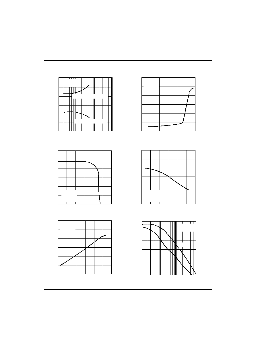
0
0.2
1
0.4
Io- Output(Sink)Current -mA
0.6
1.5
2
0.5
0
0
0.6
fosc -Oscillator Frequency -Hz
Figure 11 PWM Triangle Wave Amplitude Voltage
vs Oscillator Frequency
100k
1M
10k
0.3
2.5
3
V
o
-
E
r
r
o
r
A
m
p
l
i
f
i
e
r
O
u
t
p
u
t
V
o
l
t
a
g
e
-
V
Figure 12 Error Amplifier Output Voltage
vs Output(Sink)Current
-25
25
75
-50
0
2.42
50
T
A
-Ambient Temperature-∞C
100
2.43
2.44
2.41
2.40
2.45
2.46
Figure 14 Error Amplifier Output Voltage
vs Ambient Temperature
-25
25
75
-50
0
160
50
T
A
-Ambient Temperature-∞C
100
180
200
140
120
220
240
P
W
M
T
r
i
a
n
c
l
e
W
a
v
e
A
m
p
l
i
t
u
d
e
V
o
l
t
a
g
e
-
V
10M
0.9
1.2
1.5
1.8
V
osc
max(100% duty cycle)
V
osc
min(zero duty cycle)
Vcc=6V
T
A
=25∞C
Vcc=6V
T
A
=25∞C
V
I(FB)
=1.2V
0
40
1
80
Io- Output(Source)Current -uA
120
1.5
2
0.5
0
2.5
3
V
o
-
E
r
r
o
r
A
m
p
l
i
f
i
e
r
O
u
t
p
u
t
V
o
l
t
a
g
e
-
V
Figure 13 Error Amplifier Output Voltage
vs Output(Source)Current
20
60
100
Vcc=6V
T
A
=25∞C
V
I(FB)
=0.8V
V
o
-
E
r
r
o
r
A
m
p
l
i
f
i
e
r
O
u
t
p
u
t
V
o
l
t
a
g
e
-
V
Vcc=6V
V
I(FB)
=0.8V
No Load
Vcc=6V
V
I(FB)
=1.2V
No Load
V
o
-
E
r
r
o
r
A
m
p
l
i
f
i
e
r
O
u
t
p
u
t
V
o
l
t
a
g
e
-
V
Figure 15 Error Amplifier Output Voltage
vs Ambient Temperature
-20
0
f - Frequency -Hz
Figure 16 Error Amplifier Open-Loop Gain and
Phase Shift vs Frequency
100k
1M
10k
-10
A
v
-
E
r
r
o
r
A
m
p
l
i
f
i
e
r
O
p
e
n
-
L
oo
p
G
a
i
n
-
d
B
10M
10
20
30
40
Vcc=6V
T
A
=25∞C
Av
-180∞
-210∞
-240∞
-270∞
-300∞
-330∞
-360∞
A
v
-
E
r
r
o
r
A
m
p
l
i
f
i
e
r
O
p
e
n
-
L
o
o
p
G
a
i
n
-
d
B

UTC TL5001
LINEAR INTEGRATED CIRCUIT
UTC
UNISONIC TECHNOLOGIES CO., LTD.
10
QW-R103-016,A
-25
25
75
-50
0
50
Io -Output(Sink)Current -mA
100
1.5
0.5
0
2
Figure 20 Output Saturation Voltage
vs Output (Sink) Current
0
-20
-20
-40
Io- RT Output Current -A
-60
-30
-40
-10
0
-50
-60
Figure 19 DTC Output Current
vs RT Output Current
-10
-30
-50
T
A
=25
DT Voltage =1.3V
V
C
E
-
O
u
t
p
u
t
S
a
t
u
r
a
t
i
o
n
V
o
l
t
a
g
e
-
V
0
0.5
40
1
DTC Voltage -V
1.5
60
80
20
0
100
120
O
u
t
p
u
t
D
u
t
y
C
y
c
l
e
-
%
Figure 17 Output Duty Cycle
vs DTC Voltage
Vcc=6V
T
A
=25
Rt =100
2
20
60
100
0
40
4
80
Cscp-scp Capacitance -nF
120
6
8
2
0
10
12
t
s
c
p
-
s
c
p
T
i
m
e
-
O
u
t
P
e
r
i
o
d
-
m
s
Figure 18 Scp-Time-Output Period
vs SCP Capacitance
Vcc=6V
T
A
=25
Rt =100
DT Resistance =200k
Io
(
D
T
)
-
D
T
C
O
u
tpu
t
C
u
r
r
en
t -
A
1
Vcc=6V
T
A
=25

UTC TL5001
LINEAR INTEGRATED CIRCUIT
UTC
UNISONIC TECHNOLOGIES CO., LTD.
11
QW-R103-016,A
APPLICATION INFORMATION