UTC BT131
TRIAC
UTC
UNISONIC TECHNOLOGIES CO., LTD.
1
QW-R401-001,A
TRIACS LOGIC LEVEL
DESCRIPTION
Passivated, sensitive gate triaces in a plastic envelope,
intended for use in general purpose bidirectional switching
and phase control applications. These devices are
intended to be interfaced directly to microcontrollers. logic
integrated circuits and other low power gate trigger circuits.
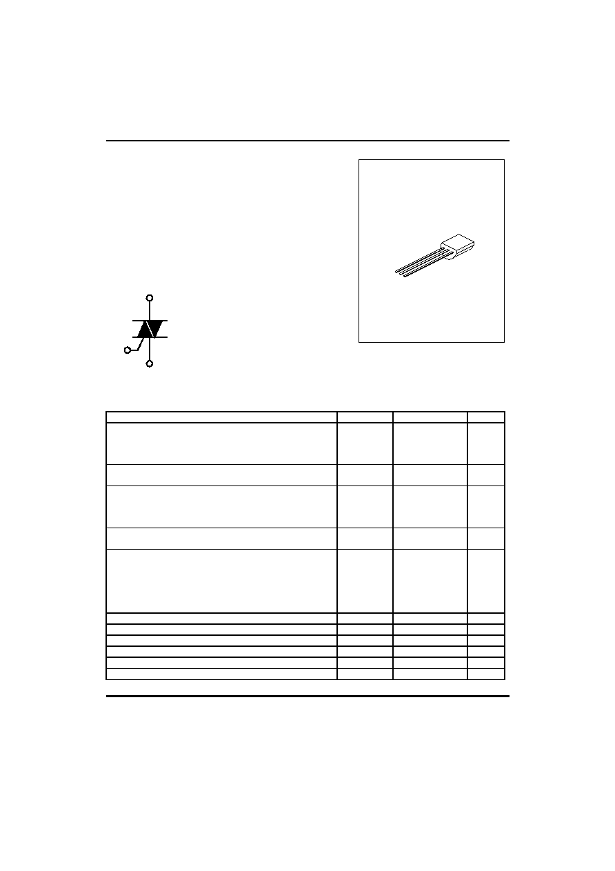
SYMBOL
MT2
MT1
G
TO-92
1
1:MT1 2:GATE 3:MT2
ABSOLUTE MAXIMUM RATINGS
PARAMETER SYMBOL
RATINGS
UNIT
Repetitive Peak Off-State Voltage
BT131-500
BT131-600
BT131-800
V
DRM
500*
600*
800*
V
RMS On-State Current
Full Sine Wave; Tlead51
�C
I
T(RMS)
1 A
Non-Repetitive Peak On-State Current
(Full Sine Wave; Tj=25
�C prior to surge)
t=20ms
t=16.7ms
I
TSM
16
17.6
A
Circuit Fusing
t=10ms
I
2
t
1.28 A
2
s
Repetitive Rate of Rise of On-State Current after Triggering
ITM=1.5A, IG=0.2A, dI
G
/dt=0.2A/
�s
T2+G+
T2+G-
T2-G-
T2-G+
dI
T
/dt
50
50
50
10
A/
�s
Peak Gate Voltage
V
GM
5 V
Peak Gate Current
I
GM
2
A
Peak Gate Power
P
GM
5
W
Average Gate Power (over any 20ms period)
P
G(AV)
0.5 W
Operating Junction Temperature
Tj
125
�C
Storage temperature
Tstg
-40~150
�C
UTC BT131
TRIAC
UTC
UNISONIC TECHNOLOGIES CO., LTD.
2
QW-R401-001,A
*Although not recommended, off-state voltages up to 800V may be applied without damage, but the triac may switch
to the on-state. The rate of rise of current should not exceed 3 A/
�s.
THERMAL RESISTANCES
PARAMETER SYMBOL
MIN
TYP
MAX
UNIT
Thermal Resistance Junction to Lead
Full Cycle
Half Cycle
Rth j-lead
60
80
K/W
Thermal Resistance junciton to Ambient
(PCB mounted ;lead length=4mm)
Rth j-lead
150 K/W
ELECTRICAL CHARACTERISTICS
(Tj=25
�C,unless otherwise specified)
PARAMETER SYMBOL
TEST
CONDITIONS
MIN
TYP
MAX
UNIT
STATIC CHARACTERISTICS
Gate Trigger Current
I
GT
V
D
=12V, I
T
=0.1A
T2+G+
T2+G-
T2-G-
T2-G+
0.4
1.3
1.4
3.8
3
3
3
7
mA
Latching Current
I
L
V
D
=12V, I
GT
=0.1A
T2+G+
T2+G-
T2-G-
T2-G+
1.2
4.0
1.0
2.5
5
8
5
8
mA
On-State Voltage Latching Current
V
T
I
T
=2.0A
1.2
1.5
V
Gate Trigger Voltage
V
GT
V
D
=12V, I
T
=0.1A
V
D
=400V, I
T
=0.1A, Tj=125
�C
0.2
0.7
0.3
1.5
V
Off-state Leakage Current
I
D
V
D
=V
DRM(max),
Tj=125
�C
0.1
0.5
mA
DYNAMIC CHARACTERISTICS
Holding Current
I
H
V
D
=12V, I
GT
=0.1A
1.3
5
mA
Critical Rate of Rise ofoff-state Voltage
dV
D
/dt V
DM
=67% V
DRM(max)
, Tj=125
�C
Exponential waveform,R
GK
=1k
5 15 V/
�s
Gate Controlled Turn-on Time
t
gt
I
TM
=1.5A,V
D
=V
DRM(max),
I
G
=0.1A
dI
G
/dt=5A/
�s
2
�s

UTC BT131
TRIAC
UTC
UNISONIC TECHNOLOGIES CO., LTD.
3
QW-R401-001,A
TYPICAL CHARACTERISTICS
1ms
100us
10us
1000
T/s
Figure 2. Maximum Permissible Non-repetitive
Peak On-state Current I
TSM
,vs Pulse Width
t
p
,for Sinusoidal Currents,t
p
20ms
10
100
1
0.4
0.6
0.8
0.2
0
1.4
0.4
IT(RMS)/A
Figure 1.Maximum on -state Dissipation.Ptot vs RMS On-
state Current,IT(RMS),Where
=conduction Angle.
1
0
1.2
1.2
0.8
0.6
0.2
10ms
100ms
100
150
-50
50
0
1.2
0.4
Tsp/
0.8
1
0.6
0.2
0
104
119
110
125
107
113
116
122
Ptot/W
Tsp(max)/C
=180
=120
=90
=60
=30
Figure 4.Maximum Permissible RMS Current I
T(RMS)
vs Lead Temperature T
lead
IT(RMS)/A
108
ITSM/A
I
T
I
TSM
time
Tj initial=25
max
dI
T
/dt limit
T2-G+ quadrant
3
1
Surge Duration /S
2.0
2.5
1.5
0.5
0
Figure 5.Maximum Permissible Repetitive RMS on-state
Current IT(RMS),vs Surge Duration,for Sinusoidal
Currents,f=50Hz;Tlead
51
IT(RMS)/A
0.01
0.1
1
10
12
4
Number of Cycles at 50Hz
8
10
6
2
0
Figure 3 .Maximum Permissible Non-Repetitive
peak on-state Current I
TSM
,vs Number of Cycles,
for Sinusoidal Currents,f=50Hz
10
100
ITSM/A
1
1000
I
T
time
I
TSM
Tj initial=25
max
100
150
-50
50
0
1.6
0.8
Tj/
1.2
1.4
1
0.6
0.4
Figure 6.Normalised Gate Trigger Voltage V
GT
(Tj)/
V
GT
(25
),vs Junction Temperature Tj
V
GT
(25
)
V
GT
(Tj
)

UTC BT131
TRIAC
UTC
UNISONIC TECHNOLOGIES CO., LTD.
4
QW-R401-001,A
1ms
0.1ms
10us
1
tp/s
Figure 11.Transient Thermal Impedance
Zth j-lead,vs Pulse W idth tp
0.01
0.1
10ms
0.1s
1.5
2
0
1
0.5
2
VT/V
1.5
1
0.5
0
Figure 10.Typical and Maximum
On-state Characteristic
IT/A
Tj=125
Zth j-sp(K/W )
100
150
-50
50
0
3
1
Tj/
2
2.5
1.5
.5
0
Figure 7.Normalised Gate Trigger current
I
GT
(Tj)/I
GT
(25
),vs Junction Temperature Tj
I
GT
(25
)
I
GT
(Tj
)
T2+G+
T2+G-
T2-G-
T2-G+
Tj=25
Vo=1.0V
Rs=0.21Ohms
typ
max
100
150
-50
50
0
3
1
Tj/
2
2.5
1.5
.5
0
Figure 8.Normalised Latching Current
I
L
(Tj)/I
L
(25
),vs Junction Temperature Tj
I
L
(25
)
I
L
(Tj
)
100
150
-50
50
0
3
1
Tj/
2
2.5
1.5
.5
0
Figure 9.Normalised Holding Current
I
H
(Tj)/I
H
(25
),vs Junction Temperature Tj
I
H
(25
)
I
H
(Tj
)
1s
10s
10
100
unidirectional
bidirectional
tp
t
P
D
100
150
50
0
1000
10
Tj/
100
1
Figure 12.Typical Critical Rate of Rise of off-state Voltage,
dV
D
/dt vs Junction Temperature Tj
dV
D
/dt(V/us)