2N4403
Vishay Semiconductors
formerly General Semiconductor
Document Number 88118
www.vishay.com
08-May-02
1
New Product
Small Signal Transistor (PNP)
Features
∑ PNP Silicon Epitaxial Planar Transistor for
switching and amplifier applications.
∑ As complementary type, the NPN transistor
2N4401 is recommended.
∑ On special request, this transistor is also
manufactured in the pin configuration TO-18.
∑ This transistor is also available in the SOT-23 case
with the type designation MMBT4403.
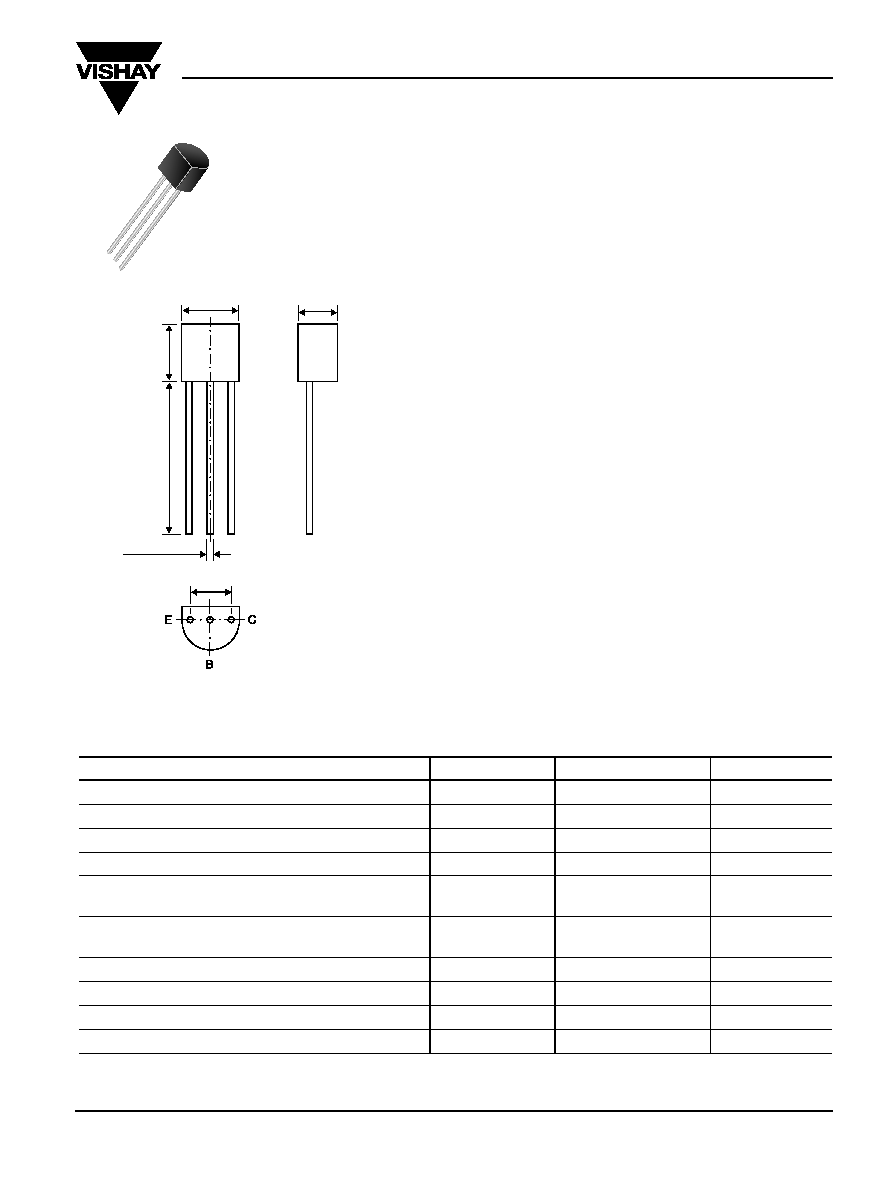
Mechanical Data
Case: TO-92 Plastic Package
Weight: approx. 0.18g
Packaging Codes/Options:
E6/Bulk ≠ 5K per container, 20K/box
E7/4K per Ammo mag., 20K/box
Maximum Ratings & Thermal Characteristics
Ratings at 25∞C ambient temperature unless otherwise specified.
Parameter
Symbol
Value
Unit
Collector-Emitter Voltage
≠V
CEO
40
V
Collector-Base Voltage
≠V
CBO
40
V
Emitter-Base Voltage
≠V
EBO
5.0
V
Collector Current
≠I
C
600
mA
Power Dissipation
T
A
= 25∞C
P
tot
625
mW
Derate above 25∞C
5.0
mW/∞C
Power Dissipation
T
C
= 25∞C
P
tot
1.5
W
Derate above 25∞C
12
mW/∞C
Thermal Resistance Junction to Ambient Air
R
JA
200
∞C/W
Thermal Resistance Junction to Case
R
JC
83.3
∞C/W
Junction Temperature
T
j
150
∞
C
Storage Temperature Range
T
S
≠55 to +150
∞
C
0.181 (4.6)
m
i
n
.
0.492
(12.5
)
0.1
81 (4
.6)
0.142 (3.6)
0.098 (2.5)
max.
0.022 (0.55)
Bottom
View
TO-226AA (TO-92)
Dimensions in inches
and (millimeters)
2N4403
Vishay Semiconductors
formerly General Semiconductor
www.vishay.com
Document Number 88118
2
08-May-02
Electrical Characteristics
(T
J
= 25∞C unless otherwise noted)
Parameter
Symbol
Test Condition
Min
Typ
Max
Unit
≠V
CE =
1 V, ≠I
C
= 0.1 mA
30
--
--
≠V
CE =
1 V, ≠I
C
= 1 mA
60
--
--
DC Current Gain
h
FE
≠V
CE =
1 V, ≠I
C
= 10 mA
100
--
--
--
≠V
CE =
2 V, ≠I
C
= 150 mA
100
--
300
≠V
CE =
2 V, ≠I
C
= 500 mA
20
--
--
Collector Cutoff Current
≠I
CEV
≠V
EB
= 0.4 V, ≠V
CE
= 35 V
--
--
100
nA
Base Cutoff Current
≠I
BEV
≠V
EB
= 0.4 V, ≠V
CE
= 35 V
--
--
100
nA
Collector-Emitter Saturation Voltage
(1)
≠V
CEsat
≠I
C
= 150 mA, ≠I
B
= 15 mA
--
--
0.40
V
≠I
C
= 500 mA, ≠I
B
= 50 mA
--
--
0.75
Base-Emitter Saturation Voltage
(1)
≠V
BEsat
≠I
C
= 150 mA, ≠I
B
= 15 mA
0.75
--
0.95
V
≠I
C
= 500 mA, ≠I
B
= 50 mA
--
--
1.30
Collector-Emitter Breakdown Voltage
≠V(
BR)CEO
≠I
C
= 1 mA, I
B
= 0
40
--
--
V
Collector-Base Breakdown Voltage
≠V(
BR)CBO
≠I
C
= 0.1 mA, I
E
= 0
40
--
--
V
Emitter-Base Breakdown Voltage
≠V(
BR)EBO
≠I
E
= 0.1 mA, I
C
= 0
5.0
--
--
V
Input Impedance
h
ie
≠V
CE
= 10 V, ≠I
C
= 1 mA,
1.5
--
15
k
f = 1 kHz
Voltage Feedback Ratio
h
re
≠V
CE
= 10 V, ≠I
C
= 1 mA,
0.1 ∑ 10
-4
--
8 ∑ 10
-4
--
f = 1 kHz
Current Gain-Bandwidth Product
f
T
≠V
CE
= 10 V, ≠I
C
= 20 mA
200
--
--
MHz
f = 100 MHz
Collector-Base Capacitance
C
CB
≠V
CB
= 10 V, I
E
= 0,
--
--
8.5
pF
f = 1.0 MHz
Emitter-Base Capacitance
C
EB
≠V
EB
= 0.5 V, I
C
= 0
--
--
30
pF
f = 1.0 MHz
Small Signal Current Gain
h
fe
≠V
CE
= 10 V, ≠I
C
= 1 mA
60
--
500
--
f = 1 kHz
Output Admittance
h
oe
≠V
CE
= 10 V, ≠I
C
= 1 mA
1.0
--
100
µ
S
f = 1 kHz
Notes:
(1) Pulse test: Pulse width
300
µ
s - Duty cycle
2%
2N4403
Vishay Semiconductors
formerly General Semiconductor
Document Number 88118
www.vishay.com
08-May-02
3
Electrical Characteristics
(T
J
= 25∞C unless otherwise noted)
Parameter
Symbol
Test Condition
Min
Typ
Max
Unit
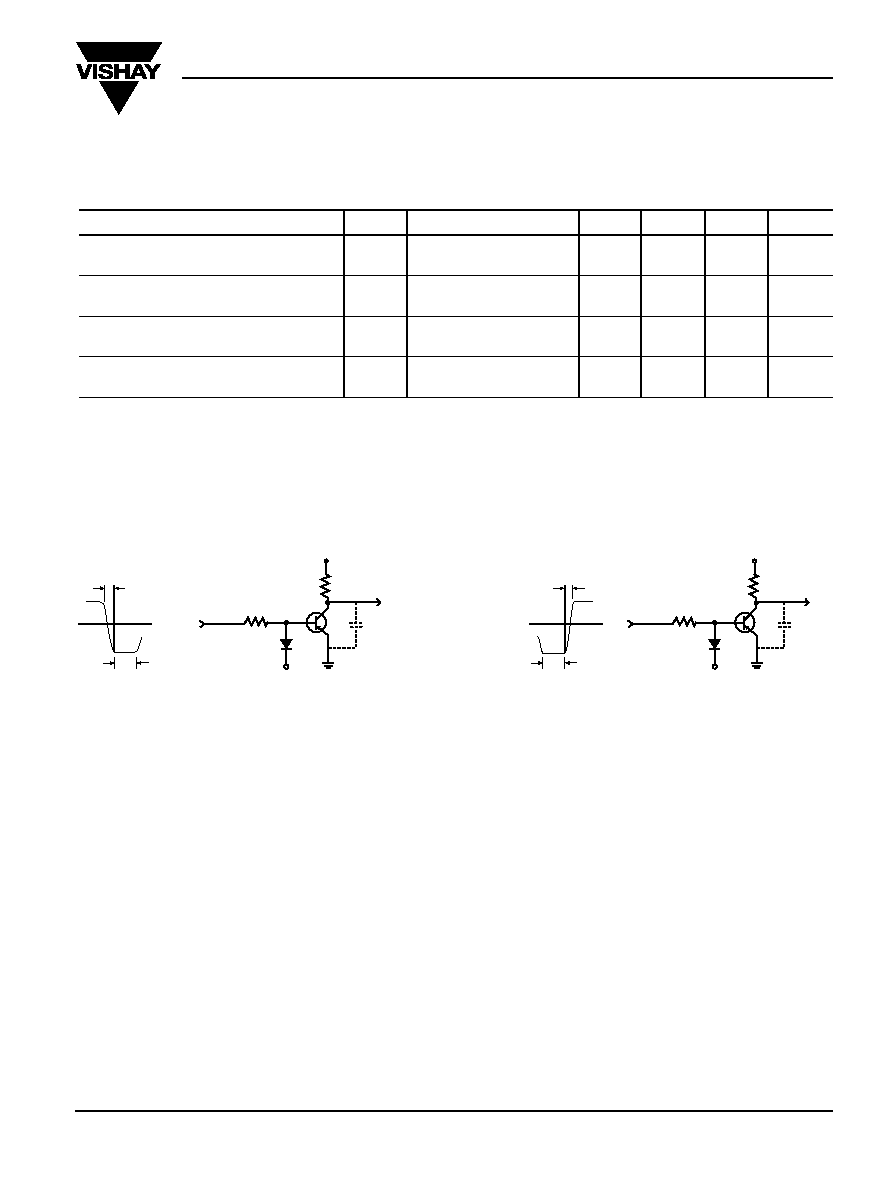
Delay Time (see fig. 1)
t
d
-I
B1
= 15 mA, -I
C
= 150 mA,
--
--
15
ns
-V
CC
= 30 V, -V
EB
= 2 V
Rise Time (see fig. 1)
t
r
-I
B1
= 15 mA, -I
C
= 150 mA,
--
--
20
ns
-V
CC
= 30 V, -V
EB
= 2 V
Storage Time (see fig. 2)
t
s
-I
B1
= -I
B2
= 15 mA,
--
--
225
ns
-I
C
= 150 mA, -V
CC
= 30 V
Fall Time (see fig. 2)
t
f
-I
B1
= -I
B2
= 15 mA,
--
--
30
ns
-I
C
= 150 mA, -V
CC
= 30 V
1.0 to 100
µ
s Duty Cycle - 2%
0
200
< 20 ns
-30V
+14 V
-16 V
+4 V
1.0 to 100
µ
s Duty Cycle - 2%
0
C < 10 pF
S*
200
< 2 ns
-30V
+2 V
-16 V
+4 V
1k
1k
Scope rise time - 4ns
*Total shunt capacitance of test jig,
connectors and oscilloscope
C < 10 pF
S
*
Switching Time Equivalent Test Circuit
Figure 1 - Turn-On Time
Figure 2 - Turn-Off Time