 | –≠–ª–µ–∫—Ç—Ä–æ–Ω–Ω—ã–π –∫–æ–º–ø–æ–Ω–µ–Ω—Ç: 2N5565 | –°–∫–∞—á–∞—Ç—å:  PDF PDF  ZIP ZIP |
2N5564/5565/5566
Vishay Siliconix
Document Number: 70254
S-04031--Rev. D, 04-Jun-01
www.vishay.com
8-1
Matched N-Channel JFET Pairs
PRODUCT SUMMARY
Part Number
V
GS(off)
(V)
V
(BR)GSS
Min (V)
g
fs
Min (mS)
I
G
Typ (pA)
j
V
GS1
≠ V
GS2
j
Max (mV)
2N5564
≠0.5 to ≠3
≠40
7.5
≠3
5
2N5565
≠0.5 to ≠3
≠40
7.5
≠3
10
2N5566
≠0.5 to ≠3
≠40
7.5
≠3
20
FEATURES
BENEFITS
APPLICATIONS
D
Two-Chip Design
D
High Slew Rate
D
Low Offset/Drift Voltage
D
Low Gate Leakage: 3 pA
D
Low Noise: 12
nV
/
Hz
@ 10 Hz
D
Good CMRR: 76 dB
D
Minimum Parasitics
D
Tight Differential Match vs. Current
D
Improved Op Amp Speed, Settling Time
Accuracy
D
Minimum Input Error/Trimming Requirement
D
Insignificant Signal Loss/Error Voltage
D
High System Sensitivity
D
Minimum Error with Large Input Signals
D
Maximum High Frequency Performance
D
Wideband Differential Amps
D
High-Speed,
Temp-Compensated,
Single-Ended Input Amps
D
High-Speed Comparators
D
Impedance Converters
D
Matched Switches
DESCRIPTION
The 2N5564/5565/5566 are matched pairs of JFETs mounted
in a TO-71 package. This two-chip design reduces parasitics
for good performance at high frequency while ensuring
extremely tight matching. This series features high
breakdown voltage (V
(BR)DSS
typically > 55 V), high gain
(typically > 9 mS), and <5 mV offset between the two die.
The hermetically-sealed TO-71 package is available with full
military processing (see Military Information).
For similar products see the low-noise U/SST401 series, and
the low-leakage 2N5196/5197/5198/5199 data sheets.
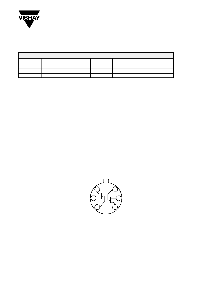
TO-71
Top View
G
1
S
1
D
1
G
2
D
2
S
2
1
2
3
6
5
4
ABSOLUTE MAXIMUM RATINGS
Gate-Drain, Gate-Source Voltage
≠40 V
. . . . . . . . . . . . . . . . . . . . . . . . . . . . . . .
Gate-Gate Voltage
"
80 V
. . . . . . . . . . . . . . . . . . . . . . . . . . . . . . . . . . . . . . . . . . . .
Gate Current
50 mA
. . . . . . . . . . . . . . . . . . . . . . . . . . . . . . . . . . . . . . . . . . . . . . . . .
Lead Temperature (
1
/
16
" from case for 10 sec.)
300
_
C
. . . . . . . . . . . . . . . . . .
Storage Temperature
≠65 to 200
_
C
. . . . . . . . . . . . . . . . . . . . . . . . . . . . . . . . . . .
Operating Junction Temperature
≠55 to 150
_
C
. . . . . . . . . . . . . . . . . . . . . . . . . .
Power Dissipation :
Per Side
a
325 mW
. . . . . . . . . . . . . . . . . . . . . . . .
Total
b
650 mW
. . . . . . . . . . . . . . . . . . . . . . . . . . .
Notes
a.
Derate 2.6 mW/
_
C above 25
_
C
b.
Derate 5.2 mW/
_
C above 25
_
C

2N5564/5565/5566
Vishay Siliconix
www.vishay.com
8-2
Document Number: 70254
S-04031--Rev. D, 04-Jun-01
SPECIFICATIONS (T
A
= 25_C UNLESS OTHERWISE NOTED)
Limits
2N5564
2N5565
2N5566
Parameter
Symbol
Test Conditions
Typ
a
Min
Max
Min
Max
Min
Max
Unit
Static
Gate-Source
Breakdown Voltage
V
(BR)GSS
I
G
= ≠1
m
A, V
DS
= 0 V
≠55
≠40
≠40
≠40
Gate-Source
Cutoff Voltage
V
GS(off)
V
DS
= 15 V, I
D
= 1 nA
≠2
≠0.5
≠3
≠0.5
≠3
≠0.5
≠3
V
Saturation Drain
Current
b
I
DSS
V
DS
= 15 V, V
GS
= 0 V
20
5
30
5
30
5
30
mA
V
GS
= ≠20 V, V
DS
= 0 V
≠5
≠100
≠100
≠100
pA
Gate Reverse Current
I
GSS
T
A
= 150
_
C
≠10
≠200
≠200
≠200
nA
V
DG
= 15 V, I
D
= 2 mA
≠3
pA
Gate Operating Current
c
I
G
T
A
= 125
_
C
≠1
nA
Drain-Source
On-Resistance
r
DS(on)
V
GS
= 0 V, I
D
= 1 mA
50
100
100
100
W
Gate-Source Voltage
c
V
GS
V
DG
= 15 V, I
D
= 2 mA
≠1.2
Gate-Source
Forward Voltage
V
GS(F)
I
G
= 2 mA , V
DS
= 0 V
0.7
1
1
1
V
Dynamic
Common-Source
Forward Transconductance
g
fs
V
DS
= 15 V, I
D
= 2 mA
9
7.5
12.5
7.5
12.5
7.5
12.5
mS
Common-Source
Output Conductance
g
os
V
DS
= 15 V, I
D
= 2 mA
f = 1 kHz
35
45
45
45
m
S
Common-Source
Forward Transconductance
g
fs
V
DS
= 15 V, I
D
= 2 mA
f = 100 MHz
8.5
7
7
7
mS
Common-Source
Input Capacitance
C
iss
10
12
12
12
Common-Source
Reverse Transfer
Capacitance
C
rss
V
DS
= 15 V, I
D
= 2 mA
f = 1 MHz
2.5
3
3
3
pF
Equivalent Input
Noise Voltage
e
n
V
DS
= 15 V, I
D
= 2 mA
f = 10 Hz
12
50
50
50
nV
/
Hz
Noise Figure
NF
R
G
= 10 M
W
1
1
1
dB
Matching
Differential
Gate-Source Voltage
|V
GS1
≠V
GS2
|
V
DG
= 15 V, I
D
= 2 mA
5
10
20
mV
Gate-Source Voltage
Differential Change
with Temperature
D
|V
GS1
≠V
GS2
|
D
T
V
DG
= 15 V, I
D
= 2 mA
T
A
= ≠55 to 125
_
C
10
25
50
m
V/
_
C
Saturation Drain
Current Ratio
c
I
DSS1
I
DSS2
V
DS
= 15 V, V
GS
= 0 V
0.98
0.95
1
0.95
1
0.95
1
Transconductance Ratio
g
fs1
g
fs2
V
DS
= 15 V, I
D
= 2 mA
f = 1 kHz
0.98
0.95
1
0.90
1
0.90
1
Common Mode
Rejection Ratio
c
CMRR
V
DG
= 10 to 20 V
I
D
= 2 mA
76
dB
Notes
a.
Typical values are for DESIGN AID ONLY, not guaranteed nor subject to production testing.
NCBD
b.
Pulse test: PW
v
300
m
s duty cycle
v
3%.
c.
This parameter not registered with JEDEC.
2N5564/5565/5566
Vishay Siliconix
Document Number: 70254
S-04031--Rev. D, 04-Jun-01
www.vishay.com
8-3
TYPICAL CHARACTERISTICS (T
A
= 25_C UNLESS OTHERWISE NOTED)
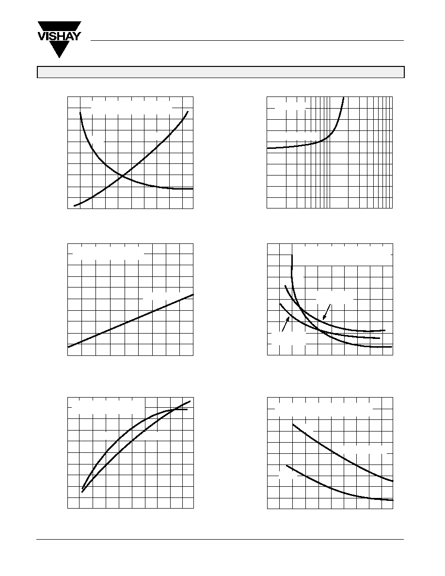
On-Resistance and Drain Current
vs. Gate-Source Cutoff Voltage
On-Resistance vs. Drain Current
100
0
≠10
0
200
160
0
r
DS
I
DSS
r
DS
@ ID = 1 mA, V
GS
= 0
I
DSS
@ V
DS
= 15 V, V
GS
= 0
100
0
1
10
100
V
GS(off)
= ≠2 V
T
A
= 25
_
C
V
GS(off)
≠ Gate-Source Cutoff Voltage (V)
I
D
≠ Drain Current (mA)
80
60
40
20
80
60
40
20
≠2
≠4
≠6
≠8
120
80
40
Turn-On Switching
5
0
≠10
4
3
2
1
0
t
r
Switching T
ime
(ns)
t
d(on)
@
I
D
= 3 mA
t
d(on)
@
I
D
= 12 mA
t
r
approximately independent of I
D
V
DG
= 5 V, R
G
= 50
W
V
GS(L)
= ≠10 V
V
GS(off)
≠ Gate-Source Cutoff Voltage (V)
≠2
≠4
≠6
≠8
Turn-Off Switching
30
0
10
24
18
12
6
0
V
GS(off)
= ≠2 V
t
d(off)
t
d(off)
independent of device V
GS(off)
V
DG
= 5 V, V
GS(L)
= ≠10 V
I
D
≠ Drain Current (mA)
2
4
6
8
Switching T
ime
(ns)
Forward Transconductance and Output Conductance
vs. Gate-Source Cutoff Voltage
50
0
0
≠2
≠10
500
200
0
g
fs
≠
Forward
T
ransconductance (mS)
g
fs
g
os
g
fs
and g
os
@ V
DS
= 15 V
V
GS
= 0 V, f = 1 kHz
V
GS(off)
≠ Gate-Source Cutoff Voltage (V)
40
30
20
10
≠4
≠6
≠8
400
200
100
160
120
On-Resistance vs. Temperature
200
≠55
25
125
0
≠15
85
I
D
= 1 mA
r
DS
changes 0.7%/
_
C
V
GS(off)
= ≠2 V
T
A
≠ Temperature (
_
C)
80
40
≠35
5
45
65
105
t
f
r
DS(on)
≠
Drain-Source On-Resistance (
)
W
r
DS(on)
≠
Drain-Source On-Resistance (
)
W
r
DS(on)
≠
Drain-Source On-Resistance (
)
W
≠
Saturation Drain Current (mA)
I
DSS
S)
g
os
≠
Output Conductance (
m
2N5564/5565/5566
Vishay Siliconix
www.vishay.com
8-4
Document Number: 70254
S-04031--Rev. D, 04-Jun-01
TYPICAL CHARACTERISTICS (T
A
= 25_C UNLESS OTHERWISE NOTED)
40
32
24
16
8
0
0
≠0.4
≠0.8
≠1.2
≠1.6
≠2
V
DS
= 15 V
≠
Drain Current (mA)
I
D
V
GS
≠ Gate-Source Voltage (V)
T
A
= ≠55
_
C
25
_
C
125
_
C
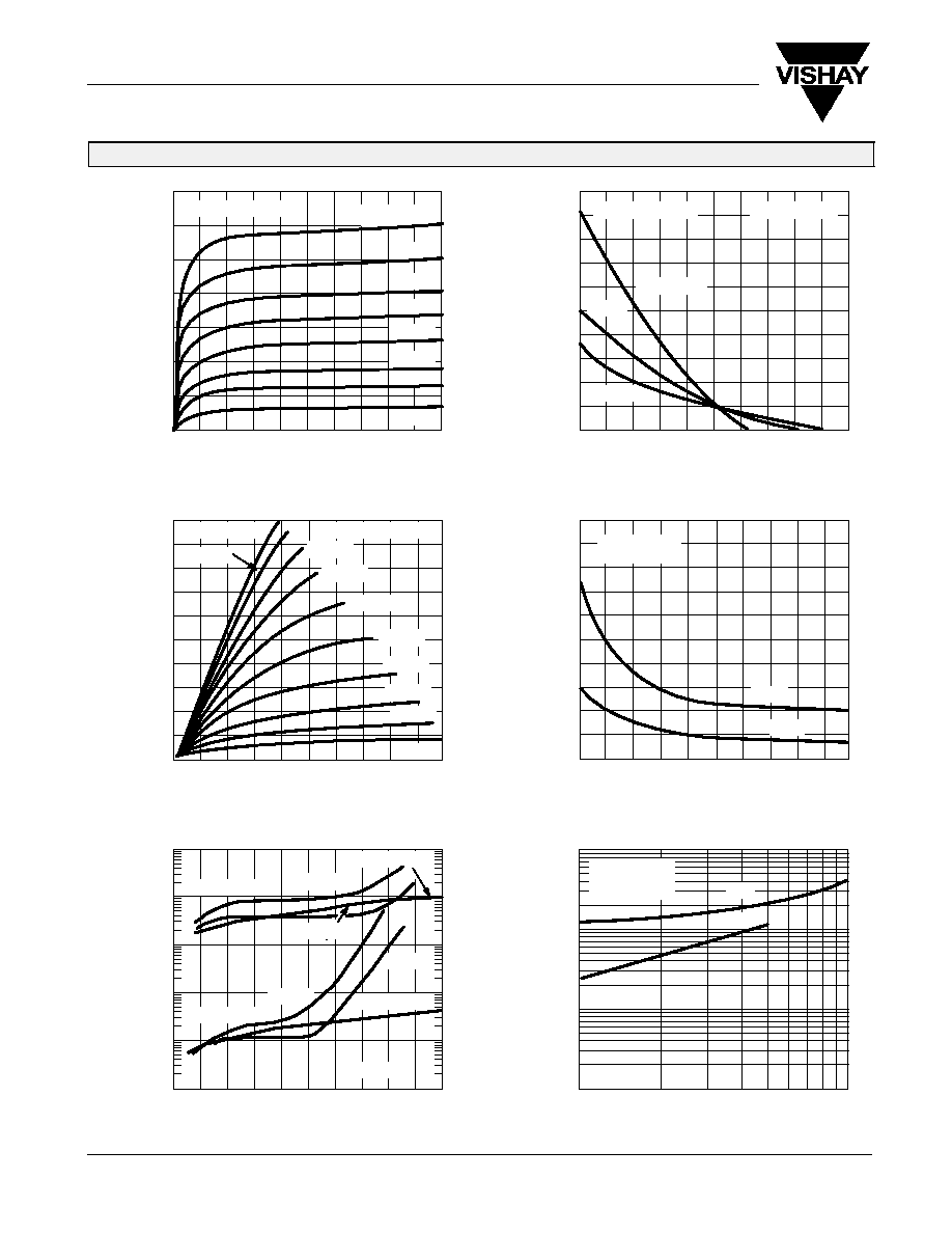
Transfer Characteristics
14
12
10
8
6
4
2
0
0
4
8
12
16
20
Output Characteristics
V
DS
≠ Drain-Source Voltage (V)
≠
Drain Current (mA)
I
D
V
GS(off)
= ≠1.5 V
V
GS
= 0 V
≠0.1 V
≠0.2 V
≠0.3 V
≠0.4 V
≠0.5 V
≠0.6 V
≠0.7 V
Output Characteristics
V
DS
≠ Drain-Source Voltage (V)
≠
Drain Current (mA)
I
D
5
0
1
0.8
0.6
0.4
0.2
4
3
2
0
1
V
GS(off)
= ≠1.5 V
≠0.2 V
≠0.3 V
≠0.4 V
≠0.5 V
≠0.6 V
≠0.7 V
≠0.8 V
≠0.9 V
Capacitance vs. Gate-Source Voltage
30
≠20
24
18
12
6
0
Capacitance (pF)
f = 1 MHz
V
DS
= 0 V
C
iss
C
rss
0
V
GS
≠ Gate-Source Voltage (V)
≠4
≠8
≠12
≠16
Gate Leakage Current
0
30
≠
Gate Leakage
I
G
T
A
= 125
_
C
T
A
= 25
_
C
1 mA
I
GSS
@ 25
_
C
I
D
= 10 mA
Common-Gate Input Admittance
100
10
1
0.1
100
1000
200
500
(mS)
g
ig
b
ig
V
DG
= 15 V
I
D
= 10 mA
T
A
= 25
_
C
V
DG
≠ Drain-Gate Voltage (V)
f ≠ Frequency (MHz)
I
GSS
@ 25
_
C
10 mA
1 mA
6
12
18
24
I
G(on)
@ I
D
0.1 pA
1 pA
10 pA
100 pA
1 nA
10 nA
≠0.1 V
V
GS(off)
= ≠2 V
V
GS
= 0 V
2N5564/5565/5566
Vishay Siliconix
Document Number: 70254
S-04031--Rev. D, 04-Jun-01
www.vishay.com
8-5
TYPICAL CHARACTERISTICS (T
A
= 25_C UNLESS OTHERWISE NOTED)
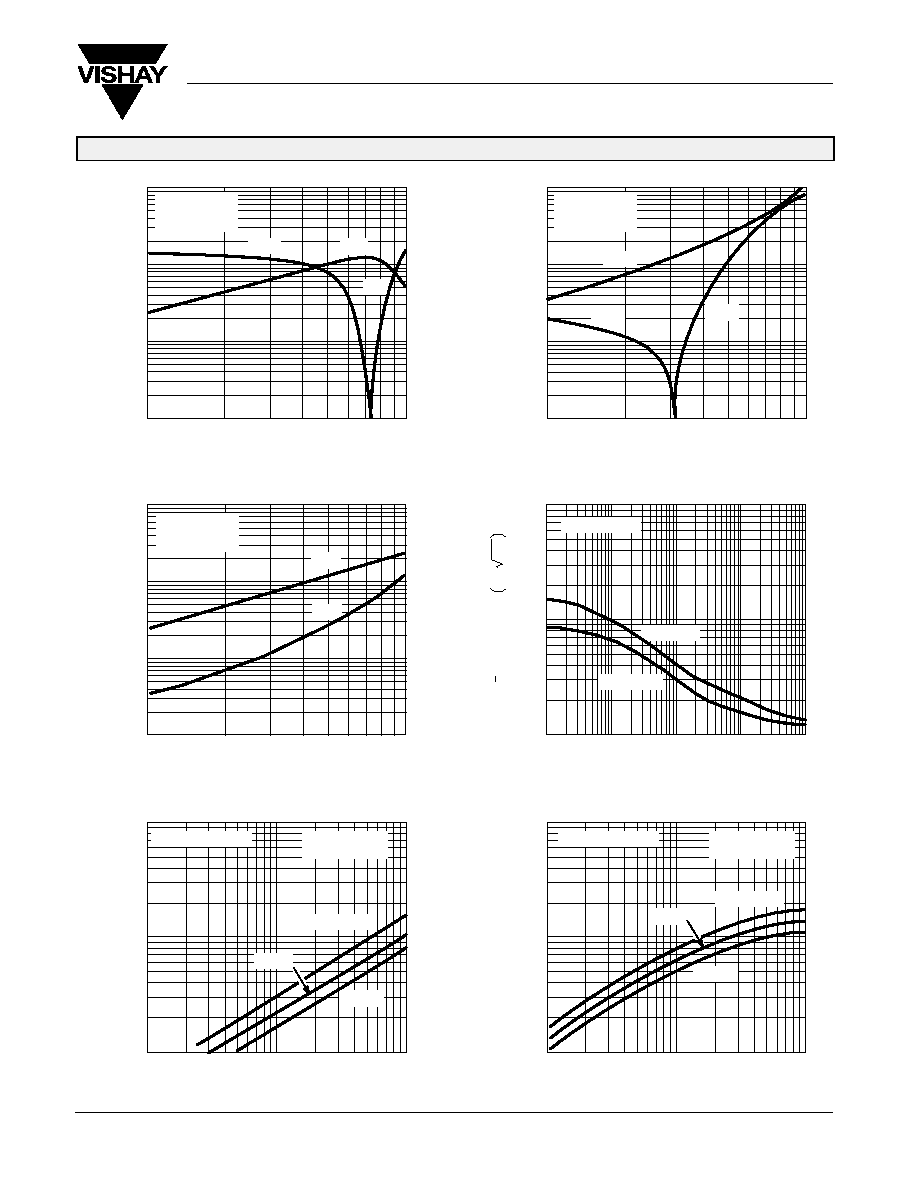
Common-Gate Forward Admittance
Common-Gate Reverse Admittance
100
10
1
0.1
100
1000
200
500
(mS)
≠g
fg
b
fg
g
fg
V
DG
= 15 V
I
D
= 10 mA
T
A
= 25
_
C
10
1
0.1
0.01
100
1000
200
500
V
DG
= 15 V
I
D
= 10 mA
T
A
= 25
_
C
≠g
rg
≠b
rg
+g
rg
(mS)
f ≠ Frequency (MHz)
f ≠ Frequency (MHz)
Common-Gate Output Admittance
100
10
1
0.1
100
1000
200
500
(mS)
V
DG
= 15 V
I
D
= 10 mA
T
A
= 25
_
C
g
og
b
og
f ≠ Frequency (MHz)
Noise Voltage vs. Frequency
100
10
1
10
100
1 k
100 k
10 k
I
D
= 1 mA
I
D
= 10 mA
V
DS
= 15 V
f ≠ Frequency (Hz)
Transconductance vs. Drain Current
100
10
1
0.1
1.0
10
I
D
≠ Drain Current (mA)
T
A
= ≠55
_
C
25
_
C
125
_
C
Output Conductance vs. Drain Current
1000
100
10
0.1
1.0
10
I
D
≠ Drain Current (mA)
T
A
= ≠55
_
C
25
_
C
125
_
C
V
DS
= 15 V
f = 1 kHz
V
GS(off)
= ≠2 V
V
DS
= 15 V
f = 1 kHz
V
GS(off)
= ≠2 V
e
n
≠
Noise V
oltage nV
/ Hz
g
os
≠
Output Conductance (
µ
S)
g
fs
≠
Forward T
ransconductance (mS)