VISHAY
BAS281 / 282 / 283
Document Number 85500
Rev. 1.6, 03-Mar-04
Vishay Semiconductors
www.vishay.com
1
9612009
Small Signal Schottky Barrier Diodes
Features
∑ Integrated protection ring against static discharge
∑ Low capacitance
∑ Low leakage current
∑ Low forward voltage drop
∑ Very low switching time
Applications
General purpose and switching Schottky barrier diode
HF-Detector
Protection circuit
Diode for low currents with a low supply voltage
Small battery charger
Power supplies
DC / DC converter for notebooks
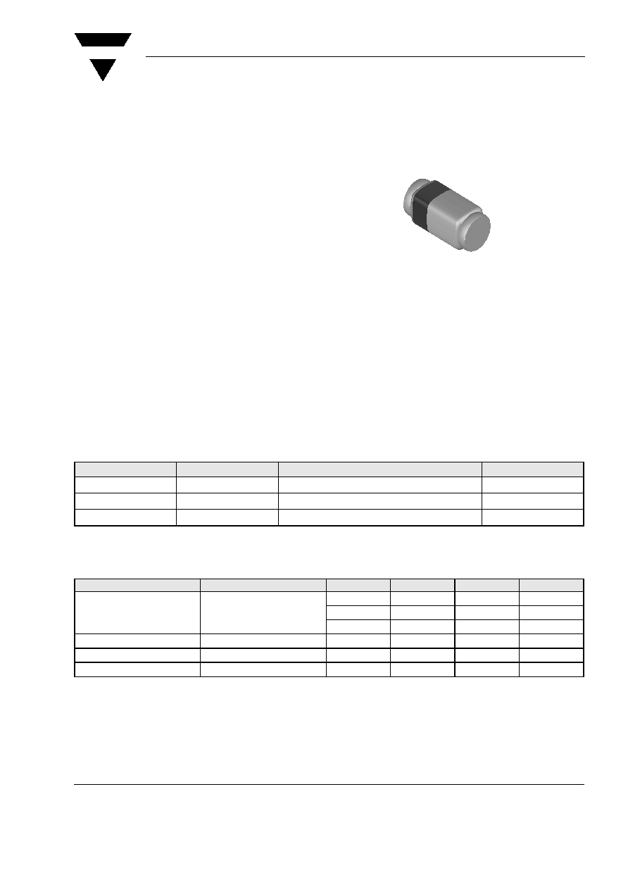
Mechanical Data
Case:QuadroMELF Glass Case (SOD-80)
Weight: approx. 33.7 mg
Cathode Band Color: Black
Packaging Codes/Options:
GS18 / 10 k per 13" reel (8 mm tape), 10 k/box
GS08 / 2.5 k per 7" reel (8 mm tape), 12.5 k/box
Parts Table
Absolute Maximum Ratings
T
amb
= 25 ∞C, unless otherwise specified
Part
Type differentiation
Ordering code
Remarks
BAS281
V
R
= 40 V
BAS281-GS18 or BAS281-GS08
Tape and Reel
BAS282
V
R
= 50 V
BAS282-GS18 or BAS282-GS08
Tape and Reel
BAS283
V
R
= 60 V
BAS283-GS18 or BAS283-GS08
Tape and Reel
Parameter
Test condition
Part
Symbol
Value
Unit
Reverse voltage
BAS281
V
R
40
V
BAS282
V
R
50
V
BAS283
V
R
60
V
Peak forward surge current
t
p
= 1 s
I
FSM
500
mA
Repetitive peak forward current
I
FRM
150
mA
Forward current
I
F
30
mA

www.vishay.com
2
Document Number 85500
Rev. 1.6, 03-Mar-04
VISHAY
BAS281 / 282 / 283
Vishay Semiconductors
Thermal Characteristics
T
amb
= 25 ∞C, unless otherwise specified
Electrical Characteristics
T
amb
= 25 ∞C, unless otherwise specified
Typical Characteristics
(T
amb
= 25
∞C unless otherwise specified)
Parameter
Test condition
Symbol
Value
Unit
Junction ambient
on PC board
50 mm x 50 mm x 1.6 mm
R
thJA
320
K/W
Junction temperature
T
j
125
∞C
Storage temperature range
T
stg
- 65 to + 150
∞C
Parameter
Test condition
Symbol
Min
Typ.
Max
Unit
Forward voltage
I
F
= 0.1 mA
V
F
330
mV
I
F
= 1 mA
V
F
410
mV
I
F
= 15 mA
V
F
1
V
Reverse current
V
R
= V
Rmax
I
R
200
nA
Diode capacitance
V
R
= 1 V, f = 1 MHz
C
D
1.6
pF
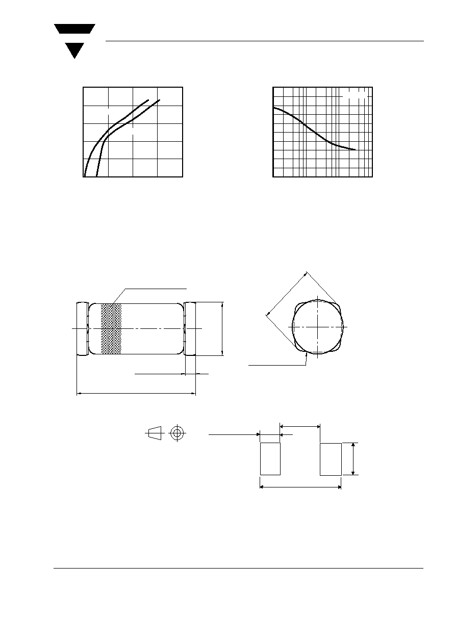
Fig. 1 Max. Reverse Power Dissipation vs. Junction Temperature
0
2
4
6
8
10
12
14
25
50
75
100
125
150
T
j
- Junction Temperature ( ∞ C )
15794
V
R
= 60 V
P
-
Reverse
Power
Dissipation
(
m
W
)
R
R
= 540 K/W
thJA
P
R
V
R
- Limit @ 100 %
P
R
V
R
- Limit @ 80 %
Fig. 2 Reverse Current vs. Junction Temperature
0.1
100
1000
25
50
75
100
125
150
1
10
15795
V
R
= V
RRM
i
I
-
Reverse
Current
(
µ
A)
R
T
j
- Junction Temperature ( ∞ C )

www.vishay.com
4
Document Number 85500
Rev. 1.6, 03-Mar-04
VISHAY
BAS281 / 282 / 283
Vishay Semiconductors
Ozone Depleting Substances Policy Statement
It is the policy of Vishay Semiconductor GmbH to
1. Meet all present and future national and international statutory requirements.
2. Regularly and continuously improve the performance of our products, processes, distribution and
operatingsystems with respect to their impact on the health and safety of our employees and the public, as
well as their impact on the environment.
It is particular concern to control or eliminate releases of those substances into the atmosphere which are
known as ozone depleting substances (ODSs).
The Montreal Protocol (1987) and its London Amendments (1990) intend to severely restrict the use of ODSs
and forbid their use within the next ten years. Various national and international initiatives are pressing for an
earlier ban on these substances.
Vishay Semiconductor GmbH has been able to use its policy of continuous improvements to eliminate the
use of ODSs listed in the following documents.
1. Annex A, B and list of transitional substances of the Montreal Protocol and the London Amendments
respectively
2. Class I and II ozone depleting substances in the Clean Air Act Amendments of 1990 by the Environmental
Protection Agency (EPA) in the USA
3. Council Decision 88/540/EEC and 91/690/EEC Annex A, B and C (transitional substances) respectively.
Vishay Semiconductor GmbH can certify that our semiconductors are not manufactured with ozone depleting
substances and do not contain such substances.
We reserve the right to make changes to improve technical design
and may do so without further notice.
Parameters can vary in different applications. All operating parameters must be validated for each
customer application by the customer. Should the buyer use Vishay Semiconductors products for any
unintended or unauthorized application, the buyer shall indemnify Vishay Semiconductors against all
claims, costs, damages, and expenses, arising out of, directly or indirectly, any claim of personal
damage, injury or death associated with such unintended or unauthorized use.
Vishay Semiconductor GmbH, P.O.B. 3535, D-74025 Heilbronn, Germany
Telephone: 49 (0)7131 67 2831, Fax number: 49 (0)7131 67 2423